DPA422-426
overloaded output exists, the feedback loop will close, providing
external CONTROL pin current, before the CONTROL pin
voltage has had a chance to discharge to the lower threshold
voltage of approximately 4.8 V (internal supply undervoltage
lockout threshold). When the externally fed current charges the
CONTROL pin to the shunt regulator voltage of 5.8 V, current in
excess of the consumption of the chip is shunted to SOURCE
through resistor RE as shown in Figure 2. This current flowing
through RE controls the duty cycle of the power MOSFET to
provide closed loop regulation. The shunt regulator has a finite
low output impedance ZC that sets the gain of the error amplifier
when used in a primary feedback configuration. The dynamic
impedance ZC of the CONTROL pin together with the external
CONTROL pin capacitance sets the dominant pole for the
control loop.
Oscillator and Switching Frequency
The internal oscillator linearly charges and discharges an
internal capacitance between two voltage levels to create a
sawtooth waveform for the pulse width modulator. The
oscillator sets both the pulse width modulator latch and the
current limit latch at the beginning of each cycle.
The nominal switching frequency of 400 kHz was chosen to
minimize the transformer size and to allow faster power supply
loop response. The FREQUENCY pin, when shorted to the
CONTROL pin, lowers the switching frequency to 300 kHz,
which may be preferable in some applications such as those
employing secondary synchronous rectification. Otherwise, the
FREQUENCY pin should be connected to the SOURCE pin for
the default 400 kHz.
Pulse Width Modulator and Maximum Duty Cycle
When a fault condition such as an open loop or overloaded
output prevents the flow of an external current into the CONTROL
pin, the capacitor on the CONTROL pin discharges towards 4.8
V. At 4.8 V auto-restart is activated which turns the output
MOSFET off and puts the control circuitry in a low current
standby mode. The high-voltage current source turns on and
charges the external capacitance again. A hysteretic internal
supply undervoltage comparator keeps VC within a window of
typically 4.8 V to 5.8 V by turning the high-voltage current
source on and off as shown in Figure 5. The auto-restart circuit
has a divide-by-8 counter that prevents the output MOSFET
from turning on again until eight discharge/charge cycles have
elapsed. This is accomplished by enabling the output MOSFET
only when the divide-by-8 counter reaches full count (S7). The
counter effectively limits DPA-Switch power dissipation as well
as the maximum power delivered to the power supply output by
reducing the auto-restart duty cycle to typically 4%. Auto-
restart mode continues until output voltage regulation is again
achieved through closure of the feedback loop.
The pulse width modulator implements voltage mode control by
driving the output MOSFET with a duty cycle inversely
proportional to the current into the CONTROL pin that is in
excess of the internal supply current of the chip (see Figure 4).
The excess current is the feedback error signal that appears
across RE (see Figure 2). This signal is filtered by an RC network
with a typical corner frequency of 30 kHz to reduce the effect of
switching noise in the chip supply current generated by the
MOSFET gate driver. The filtered error signal is compared with
the internal oscillator sawtooth waveform to generate the duty
cycle waveform. As the control current increases, the duty cycle
decreases. A clock signal from the oscillator sets a latch that
turns on the output MOSFET. The pulse width modulator resets
the latch, turning off the output MOSFET. Note that a minimum
current must be driven into the CONTROL pin before the duty
cycle begins to change.
VUV
VLINE
0 V
S0
S0
S7
S1
S2
S6
S7 S0
S1
S2
S6
S7
S1 S2
S6
S7
S7
5.8 V
4.8 V
VC
0 V
VDRAIN
0 V
VOUT
0 V
1
3
2
2
4
Note: S0 through S7 are the output states of the auto-restart counter
PI-3867-050602
Figure 5. Typical Waveforms for (1) Power Up, (2) Normal Operation, (3) Auto-restart and (4) Power Down.
5
www.powerint.com
Rev. T 12/12


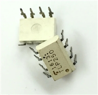
 TLP250光耦合器:资料手册参数分析

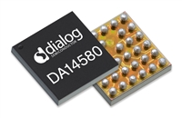
 DA14580 低功耗蓝牙系统级芯片(SoC):资料手册参数分析

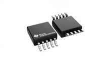
 INA226 高精度电流和功率监控器:资料手册参数分析

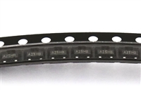
 SI2302 N沟道MOSFET:资料手册参数分析
