The Communications Edge TM
CV211-1
PCS/DCS-band Dual-Branch Downconverter
Product Information
Product Features
Product Description
Functional Diagram
• High dynamic range downconverter
with integrated LO and IF amplifiers
The CV211-1 is
a
dual-channel high-linearity
downconverter designed to meet the demanding
performance, functionality, and cost goals of current and
next generation mobile infrastructure basestations. It
provides high dynamic range performance in a low profile
surface-mount leadless package that measures 6 x 6 mm
square.
28
27
24
23
22
26
25
RF 1
INPUT
IF
• Dual channels for diversity
• +29.5 dBm Input IP3
• +10 dBm Input P1dB
• RF: 1710 – 2000 MHz
1
2
3
4
5
6
7
BIAS
GND
N/C
21
20
19
18
17
16
15
RF
GND
BIAS
GND
N/C
IF Amp 1
GND
LO
It is ideally suited for high dynamic range receiver front
ends using diversity receive channels. Functionality
includes frequency conversion & IF amplification, while
an integrated LO driver amplifier powers the passive
mixer. The MCM is implemented with reliable and
mature GaAs MESFET and InGaP HBT technology.
LO Driver Amp
IF Amp 2
• IF:
65 – 250 MHz
GND
GND
N/C
• Single supply operation (+5 V)
• 6x6 mm 28-pin QFN package
• Low-side LO configuration
RF 2
INPUT
IF
RF
8
9
12
13
14
10
11
Typical applications include frequency downconversion
used in PCS/DCS-band 2.5G and 3G mobile base
transceiver stations.
• Common footprint with other
PCS/UMTS/cellular versions
Top View
Specifications1
Parameters
Units
MHz
MHz
MHz
%
dB
dB
dBm
dBm
dBm
dB
Min
1710
1460
65
Typ
Max
2000
1935
250
Comments
RF Frequency Range
LO Frequency Range
IF Center Frequency Range
% Bandwidth around IF center frequency
SSB Conversion Gain
Gain Drift over Temp (-40° C to 85° C)
Input IP3
Input IP2
Input 1 dB Compression Point
Noise Figure
240
±7.5
10
±0.5
+29.5
+38
+10
11
See note 2
See note 3
Temp = 25° C
Referenced to +25° C
See note 4
See note 4
See note 4
See note 5
8
12
1.5
-1.5
+25
+33
LO Input Drive Level
LO-RF Isolation
LO-IF Isolation
dBm
dB
dB
-2.5
0
8
32
+2.5
PLO = 0 dBm
PLO = 0 dBm
Branch-Branch Isolation
Return Loss: RF Port
Return Loss: LO Port
Return Loss: IF Port
Operating Supply Voltage
Supply Current
dB
dB
dB
dB
45
18
15
12
+5
380
V
mA
°C / W
°C
320
475
27
160
Thermal Resistance
Junction Temperature
See note 6
1. Specifications when using the application specific circuit (shown on page 3) with a low side LO = 0 dBm in a downconverting application at 25° C.
2. IF matching components affect the center IF frequency. Proper component values for other IF center frequencies than shown can be provided by emailing to applications.engineering@wj.com.
3. The IF bandwidth of the converter is defined as 15% around any center frequency in its operating IF frequency range. The bandwidth is determined with external components. Specifications are valid around
the total ±7.5% bandwidth. ie. with a center frequency of 240 MHz, the specifications are valid from 240 ± 18 MHz.
4. Assumes the supply voltage = +5 V. IIP3 is measured with ∆f = 1 MHz with RFin = -5 dBm / tone.
5. Assumes LO injection noise is filtered at the thermal noise floor, -174 dBm/Hz, at the RF, IF, and Image frequencies.
6. The maximum junction temperature ensures a minimum MTBF rating of 1 million hours of usage.
Absolute Maximum Rating
Ordering Information
Parameters
Rating
-40° to +85° C
-55° to +125° C
+5.5 V
Part No.
Description
Operating Case Temperature
Storage Temperature
DC Voltage
CV211-1
PCS/DCS-band Dual-Branch Downconverter
CV211-1PCB240 Fully-Assembled Application Board, IF = 240 MHz
Junction Temperature
+220 °C
Operation of this device above any of these parameters may cause permanent damage.
Specifications and information are subject to change without notice
WJ Communications, Inc • Phone 1-800-WJ1-4401 • FAX: 408-577-6621 • e-mail: sales@wj.com • Web site: www.wj.com
October 2003


 BSS138LT3G:一款高效能N沟道MOSFET的全面解析

 解读EGP10B二极管资料手册:产品特性、参数分析

 RT9164AGG手册资料详解:引脚信息、设计指南

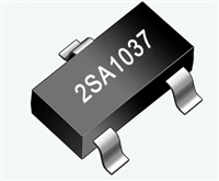
 2SA1037KPT资料详解:产品特性、电气参数、设计指南
