OUTPUT CURRENT
APPLICATION INFORMATION
The BUF634 can deliver up to ±250mA continuous output
current. Internal circuitry limits output current to approxi-
mately ±350mA—see typical performance curve “Short
Circuit Current vs Temperature”. For many applications,
however, the continuous output current will be limited by
thermal effects.
Figure 1 is a simplified circuit diagram of the BUF634
showing its open-loop complementary follower design.
V+
The output voltage swing capability varies with junction
temperature and output current—see typical curves “Output
Voltage Swing vs Output Current.” Although all four pack-
age types are tested for the same output performance using
a high speed test, the higher junction temperatures with the
DIP and SO-8 package types will often provide less output
voltage swing. Junction temperature is reduced in the DDPAK
surface-mount power package because it is soldered directly
to the circuit board. The TO-220 package used with a good
heat sink further reduces junction temperature, allowing
maximum possible output swing.
Thermal
Shutdown
200Ω
VIN
VO
(1)
I1
THERMAL PROTECTION
150Ω
4kΩ
Power dissipated in the BUF634 will cause the junction
temperature to rise. A thermal protection circuit in the
BUF634 will disable the output when the junction tempera-
ture reaches approximately 175°C. When the thermal pro-
tection is activated, the output stage is disabled, allowing the
device to cool. Quiescent current is approximately 6mA
during thermal shutdown. When the junction temperature
cools to approximately 165°C the output circuitry is again
enabled. This can cause the protection circuit to cycle on and
off with a period ranging from a fraction of a second to
several minutes or more, depending on package type, signal,
load and thermal environment.
BW
V–
Signal path indicated in bold.
Note: (1) Stage currents are set by I1.
FIGURE 1. Simplified Circuit Diagram.
Figure 2 shows the BUF634 connected as an open-loop
buffer. The source impedance and optional input resistor,
RS, influence frequency response—see typical curves. Power
supplies should be bypassed with capacitors connected close
to the device pins. Capacitor values as low as 0.1µF will
assure stable operation in most applications, but high output
current and fast output slewing can demand large current
transients from the power supplies. Solid tantalum 10µF
capacitors are recommended.
The thermal protection circuit is designed to prevent damage
during abnormal conditions. Any tendency to activate the
thermal protection circuit during normal operation is a sign
of an inadequate heat sink or excessive power dissipation for
the package type.
TO-220 package provides the best thermal performance.
When the TO-220 is used with a properly sized heat sink,
output is not limited by thermal performance. See Applica-
tion Bulletin AB-037 for details on heat sink calculations.
The DDPAK also has excellent thermal characteristics. Its
mounting tab should be soldered to a circuit board copper
area for good heat dissipation. Figure 3 shows typical
thermal resistance from junction to ambient as a function of
the copper area. The mounting tab of the TO-220 and
DDPAK packages is electrically connected to the V– power
supply.
High frequency open-loop applications may benefit from
special bypassing and layout considerations—see “High
Frequency Applications” at end of applications discussion.
V+
10µF
DIP/SO-8
Pinout shown
7
RS
VIN
3
6
The DIP and SO-8 surface-mount packages are excellent for
applications requiring high output current with low average
power dissipation. To achieve the best possible thermal
performance with the DIP or SO-8 packages, solder the
device directly to a circuit board. Since much of the heat is
dissipated by conduction through the package pins, sockets
will degrade thermal performance. Use wide circuit board
traces on all the device pins, including pins that are not
connected. With the DIP package, use traces on both sides
of the printed circuit board if possible.
VO
BUF634
1
RL
4
10µF
Optional connection for
wide bandwidth — see text.
V–
FIGURE 2. Buffer Connections.
®
7
BUF634


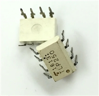
 TLP250光耦合器:资料手册参数分析

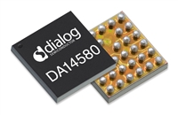
 DA14580 低功耗蓝牙系统级芯片(SoC):资料手册参数分析

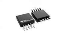
 INA226 高精度电流和功率监控器:资料手册参数分析

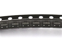
 SI2302 N沟道MOSFET:资料手册参数分析
