
 5秒后页面跳转

| 型号 | 品牌 | 描述 | 获取价格 | 数据表 |
| BD8151EFV-E2 | ROHM | Switching Regulator, Current-mode, 1.5A, 1320kHz Switching Freq-Max, PDSO20, HTSSOP-20 |
获取价格 |

|
| BD8152FVM | ROHM | TFT-LCD Bias Boost Converter |
获取价格 |
|
| BD8152FVM_1 | ROHM | High-efficiency Step-up Switching Regulators with Built-in Power MOSFET |
获取价格 |
|
| BD8152FVM_11 | ROHM | High-efficiency Step-up Switching Regulators with Built-in Power MOSFET |
获取价格 |
|
| BD8152FVM-E2 | ROHM | High-efficiency Step-up Switching Regulators with Built-in Power MOSFET |
获取价格 |
|
| BD8152FVM-TR | ROHM | 暂无描述 |
获取价格 |
|
 MAX485 RS-485/RS-422收发器资料手册参数分析

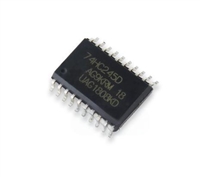 74HC245八路双向总线收发器:资料手册参数分析
 CD4053模拟多路复用器/解复用器:资料手册参数分析
 CD4011双4位二进制计数器:资料手册参数分析
工作时间:9:00-21:00
CEO邮箱:ceo@jiepei.com
投诉邮箱:tousu@jiepei.com


 浙公网安备 33010502006866号 浙ICP备10014259号-119
营业执照ICP证
浙公网安备 33010502006866号 浙ICP备10014259号-119
营业执照ICP证


