OUTPUT SPECIFICATIONS
TYPICAL CHARACTERISTICS
Item
Test conditions
Min.
Typ. Max. Units
Output power
0.25
±1.5
±1.2
20
W
For Vin change of ±1%(3.3V output)
For Vin change of ±1%(others output)
10% to 100% load(3.3V output)
10% to 100% load (5V output)
10% to 100% load (9V output)
10% to 100% load (12V output)
10% to 100% load (15V output)
Line regulation
15
12.8
8.3
6.8
6.3
15
%
Load regulation
15
15
15
Output voltage accuracy
See tolerance envelope graph
Temperature drift
Ripple & Noise*
100% full load
20MHz Bandwidth
±0.03 %/°C
50
75
mVp-p
kHz
Switching frequency Full load, nominal input
110
*Test ripple and noise by “parallel cable” method. See detailed operation instructions at Testing of
Power Converter section, application notes.
Operating Temp.(oC)
APPLICATION NOTE
RECOMMENDED CIRCUIT
1) Requirement on output load
L
L
+Vo
0V
To ensure this module can operate efficiently and reliably, During operation, the
minimum output load could not be less than 10% of the full load. If the actual output
power is very small, please connect a resistor with proper resistance at the output end in
parallel to increase the load.
Vin
Cout
Cin
DC
DC
GND
(Figure 1)
DC DC
2) Recommended circuit
If you want to further decrease the input/output ripple, an “LC” filtering network may be
connected to the input and output ends of the DC/DC converter, see (Figure 1).
It should also be noted that the inductance and the frequency of the “LC” filtering network
should be staggered with the DC/DC frequency to avoid mutual interference. However, the
capacitance of the output filter capacitor must be proper. If the capacitance is too big, a
startup problem might arise. It’s not recommended to connect any external capacitor in the
application field.
+Vo
Vin
REG
GND
0V
REG
+Vo
Vin
DC
DC
GND
0V
(Figure 2)
3) Output Voltage Regulation and Over-voltage Protection Circuit
The simplest device for output voltage regulation, over-voltage and over-current
protection is a linear voltage regulator with overheat protection that is connected to the
input or output end in series (Figure 2).
4) Overload Protection
Under normal operating conditions, the output circuit of these products has no
protection against overload. The simplest method is to connect a self-recovery fuse in
series at the input end or add a circuit breaker to the circuit.
5) No parallel connection or plug and play
The copyright and authority for the interpretation of the products are reserved by MORNSUN
Specifications subject to change without notice.
B_S(D)-W2 B/2-2012 Page 2 of 3


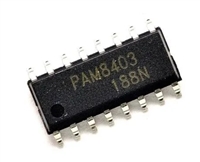
 PAM8403音频功率放大器:资料手册参数分析

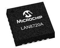
 LAN8720以太网收发器:资料手册参数分析

 SI2301 N沟道MOSFET:资料手册参数分析

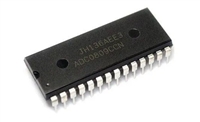
 ADC0809逐次逼近寄存器型模数转换器:资料手册参数分析
