AMIS-720341-A: Contact Image Sensor
Data Sheet
6.0 Two Test Setups for Specifications and Performance
6.1 First Setup
The standard specifications are the image sensor tests that are performed on the wafer probe machine, where each device on the
wafer is tested in production. However, the data in these measurements are measured with a clock frequency at a fixed 500kHz. Since
the pixel rate is equal to the clock rate, the pixel rate is also at 500kHz. The specification under Section 7.0 is the wafer probe
specifications, Table 2.
6.2 Second Setup
The CIS modules made with these devices operate in excess of 5.0MHz. Accordingly, the wafer probe specifications are supplemented
with high frequency clocking performance using an A6 length module’s PCB board.
7.0 Electro-Optical Characteristics (25°C)
The electro-optical characteristics of the AMIS-720341-A imaging sensor chip are listed in Table 2. This is the wafer probe specification
used to test each die at 25°C.
Table 2: Electro-Optical Characteristics
Parameters
Symbols
Typical
128
~83.3
128/Fclk
500
Units
Elements
µm
µs/line
kHz
Notes
Number of photo-elements
Pixel-to-pixel spacing
Line scanning rate
Clock frequency
(1)
Tint
Fclk (2)
See Note 2 for higher clock speed
(max. 5MHz)
Output voltage
Output voltage non-uniformity
Dark output voltage
Dark output non-uniformity
Adjacent pixel non-uniformity
Chip-to-chip non-uniformity
Notes:
Vpavg (3)
Up (4)
1.85 ± 0.35
± 7.5
V
%
mV
mV
%
(5)
Vd
Ud
<100
<100
<6.5
± 5
(6)
Upadj (7)
Ucc (8)
%
(1) Tint stands for the line scanning rate or the integration time. It is determined by the time interval between two SPs, where the SPs start the line-scan process, as
soon as the CP, module clock, acquires it and shifts it into the internal shift register. The minimum integration time in one line scan of the sensor is the number of
pixel sites divided by its clock frequency. In a CIS module it is the number of sensors times the number of pixels in the sensor, all over the clock frequency. Tint in
the wafer probe is set with the calibration procedure used to set the amplitude of Vpavg, see Note 3.
(2) Fclk is the device’s clock, CP, frequency and it is also equal to the pixel rate. In the wafer test, Fclk is set to 500kHz. However, AMIS has been successfully mass-
producing high frequency CIS modules, using only the wafer test to qualify them. Hence, the devices are constantly tested for their standard high-speed
performance with each of the A6 modules in production. These module production tests have proven that the low speed wafer probe tests are sufficient to
produce reliable image devices.
(3) Vpavg = ∑Vp(n)/Npixels (average level in one line scan)
Where Vp(n) is the amplitude of nth pixel in the sensor chip and Npixels is the total number of pixels in sensor chip.
Vpavg is converted from impulse current video pixel into a voltage output. See Figure 4, in Section 4.0. and Figure 5, in Section 5.0. There is a calibration
procedure to calibrate Vpavg using tint as the variable to control the exposure. Hence, Vpavg is calibrated for each image sensor type to compensate for the
probe card variations, as well as the interfacing circuits to the wafer probe machine.
(4) Up is the uniformity specification, measured under a uniform exposing light exposure. Up = [Vp(max) - Vpavg] / Vpavg x 100% or [Vpavg - Vp(min)] / Vpavg} x
100%, whichever is greater.
Where
Vp(max) is the maximum pixel output voltage in the light.
Vp(min) is the minimum pixel output voltage in the dark.
The pixel Vp(n) is one nth pixel in Npixels in the sensor.
(5) Vd = ∑Vp(n)/Npixels. Where Vp(n) is the pixels signal amplitude of the nth pixel of the sensor. Dark is where the light is off, leaving the image surface unexposed.
(6) Ud = Vdmax – Vdmin.
(7) Upadj = MAX[ | (Vp(n) - Vp(n+l) | / Vp(n)) x 100%. Upadj is the non-uniformity in percentage. It is the amplitude difference between two neighboring pixels.
(8) Ucc is the uniformity specifications, measured among the good die on the wafer. Under uniform light exposure the sensors are measured and calculated with the
following algorithm: Vpavg of all the good dies on the wafer are averaged and assigned VGpavg. Then the die with maximum Vpavg is assigned Vpavg(max),
and the one with minimum Vpavg is assigned Vpavg(min). Then UCC = {[Vpavg(max)-Vpavg(min)]/VGpavg}x100.
AMI Semiconductor – May 06, M-20570-001
6
www.amis.com


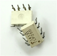
 TLP250光耦合器:资料手册参数分析

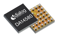
 DA14580 低功耗蓝牙系统级芯片(SoC):资料手册参数分析

 INA226 高精度电流和功率监控器:资料手册参数分析

 SI2302 N沟道MOSFET:资料手册参数分析
