ADP3154
Power Good
CT is discharged by a constant current of 65 µA. Once CT
reaches 2.3 V, a new on-time cycle is initiated. The value of the
off-time is calculated using the continuous-mode operating
The ADP3154 has an internal monitor that senses the output
voltage and drives the PWRGD pin of the device. This pin is an
open drain output whose high level (when connected to a pull-
up resistor) indicates that the output voltage has been within a
±5% regulation band of the targeted value for more than 500 µs.
The PWRGD pin will go low if the output is outside the regula-
tion band for more than 500 µs.
frequency. Assuming a nominal operating frequency of fNOM
200 kHz at an output voltage of 2.0 V, the corresponding off
time is:
=
VO
1
tOFF = 1 –
= 3.0 µs
VIN fNOM
Output Crowbar
An added feature of using an N-channel MOSFET as the syn-
chronous switch is the ability to crowbar the output with the
same MOSFET. If the output voltage is 15% greater than the
targeted value, the ADP3154 will turn on the lower MOSFET,
which will current-limit the source power supply or blow its
fuse, pull down the output voltage, and thus save the micropro-
cessor from destruction. The crowbar function releases at ap-
proximately 50% of the nominal output voltage. For example, if
the output is programmed to 2.0 V, but is pulled up to 2.3 V or
above, the crowbar will turn on the lower MOSFET. If in this
case the output is pulled down to less than 1.0 V, the crowbar
will release, allowing the output voltage to recover to 2.0 V if
the fault condition has been removed.
The timing capacitor can be calculated from the equation:
tOFF × 65 µA
CT
=
= 200 pF
1 V
The converter operates at the nominal operating frequency only
at the above specified VOUT and at light load. At higher VOUT or
heavy load, the operating frequency decreases due to the para-
sitic voltage drops across the power devices. The actual mini-
mum frequency at VOUT = 2.0 V is calculated to be 180 kHz (see
Equation 1), where:
IIN
is the input dc current
(assuming an efficiency of 90%, IIN = 7.5 A)
RIN
is the resistance of the input filter
(estimated value: 7 mΩ)
Shutdown
The ADP3154 has a shutdown (SD) pin that is pulled down by
an internal resistor. In this condition the device functions nor-
mally. This pin should be pulled high to disable the output drives.
RDS(ON)HSF
RDS(ON)LSF
RSENSE
RL
is the resistance of the high side MOSFET
(estimated value: 10 mΩ)
APPLICATION INFORMATION
Specifications for a Design Example
The design parameters for a typical 550 MHz Pentium III appli-
cation (Figure 2) are as follows:
Input voltage: VIN = 5 V
Auxiliary input: VCC = 12 V
is the resistance of the low side MOSFET
(estimated value: 10 mΩ)
is the resistance of the sense resistor
(estimated value: 5 mΩ)
is the resistance of the inductor
(estimated value: 6 mΩ)
Output voltage: VO = 2.0 V
COUT Selection–Determining the ESR
Maximum output current:
The required ESR and capacitance drive the selection of the
type and quantity of the output capacitors. The ESR must be
small enough that both the resistive voltage deviation due to a
step change in the load current and the output ripple voltage
stay below the values defined in the specification of the supplied
microprocessor. The capacitance must be large enough that the
output is held up while the inductor current ramps up or down
to the value corresponding to the new load current.
I
OMAX = 17.0 A dc
Minimum output current:
OMIN = 1.0 A dc
I
Static tolerance of the supply voltage for the processor core:
∆VOST+ = +70 mV
∆VOST– = –70 mV
Transient tolerance (for less than 2 µs) of the supply voltage for
the processor core when the load changes between the minimum
and maximum values with a di/dt of 30 A/µs:
The total static tolerance of the Pentium III processor is 140 mV.
Taking into account the ±1% setpoint accuracy of the ADP3154,
and assuming a 0.5% (or 10 mV) peak-to-peak ripple, the
allowed static voltage deviation of the output voltage when the
load changes between the minimum and maximum values is
90 mV. Assuming a step change of ∆I = IOMAX–IOMIN = 16 A,
and allocating all of the total allowed static deviation to the
contribution of the ESR sets the following limit:
∆VOTR+ = +140 mV
∆VOTR– = –140 mV
Input current di/dt when the load changes between the mini-
mum and maximum values: less than 8 A/µs.
The above requirements correspond to Intel’s published power
supply requirements based on Intel Pentium III specification
guidelines.
30 mV
16 A
RE(MAX) = ESRMAX1
=
= 5.6 mΩ
CT Selection for Operating Frequency
The output filter capacitor must have an ESR of less than 5.6 mΩ.
One can use, for example, two SP Type OS-CON capaci-
tors from Sanyo, with 2200 µF capacitance, 7 V voltage rating,
and 10 mΩ ESR. The two capacitors have a total ESR of 5.0 mΩ
when connected in parallel, which gives adequate margin.
The ADP3154 uses a constant-off-time architecture with tOFF
determined by an external timing capacitor CT. Each time the
high side N-channel MOSFET switch turns on, the voltage
across CT is reset to approximately 3.3 V. During the off time,
1
VIN – IIN RIN – IOMAX(RDS(ON)HSF + RSENSE + RL ) – VO
(1)
fMIN
=
×
= 180 kHz
tOFF VIN – IIN RIN – IOMAX(RDS(ON)HSF + RSENSE + RL – RDS(ON)LSF
)
REV. A
–7–


 深入解析AD7606高性能多通道模数转换器:资料手册参数分析

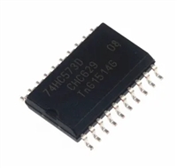
 74HC573三态非易失锁存器(Latch)资料手册参数分析

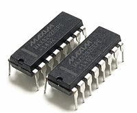
 MAX3232 RS-232电平转换器资料手册参数分析

 MAX485 RS-485/RS-422收发器资料手册参数分析
