Dual, 16-Bit, 125 MSPS Serial LVDS,
1.8 V Analog-to-Digital Converter
Data Sheet
AD9655
FUNCTIONAL BLOCK DIAGRAM
FEATURES
1.8 V supply operation
AVDD
AGND
DRVDD
Low power: approximately 150 mW/channel at 125 MSPS,
2V p-p input range (typical)
SNR/SFDR at 69.5 MHz
AD9655
D0A+
D0A–
D1A+
D1A–
D0B+
D0B–
D1B+
D1B–
DCO+
DCO–
FCO+
FCO–
16
VINA+
VINA–
16-BIT
PIPELINE
ADC
77.5 dBFS/88 dBc, 2.0 V p-p input range (typical)
79.3 dBFS/84 dBc, 2.8 V p-p input range (typical)
Linearity
DNL = 0.7 LSB; INL = 4.0 LSB (typical, 2.0 V p-p input span)
DNL = 0.7 LSB; INL = 3.4 LSB (typical, 2.8 V p-p input span)
Serial LVDS, two data lanes per ADC channel
500 MHz full power analog bandwidth
Serial port control
16
16
VCM
VINB+
VINB–
16-BIT
PIPELINE
ADC
16
REFERENCE
SERIAL PORT
INTERFACE
1 TO 8
CLOCK DIVIDER
SCLK/ SDIO/ CSB
DFS PDWN
CLK+ CLK–
Full chip and individual channel power-down modes
Flexible bit orientation
Built-in and custom digital test pattern generation
Clock divider
Figure 1.
Programmable output clock and data alignment
Standby mode
APPLICATIONS
Communications
Diversity radio systems
Multimode digital receivers
GSM, EDGE, W-CDMA, LT E, CDMA2000, WiMAX, TD-SCDMA
I/Q demodulation systems
Smart antenna systems
Broadband data applications
Battery-powered instruments
Handheld scope meters
Portable medical imaging and ultrasound
Radar/LIDAR
Individual channel power-down is supported. The AD9655
typically consumes less than 2 mW in serial port interface (SPI)
power-down mode. The available digital test pat-terns include
built-in deterministic and pseudorandom patterns, along with
custom user-defined test patterns entered via the SPI.
GENERAL DESCRIPTION
The AD9655 is available in an RoHS-compliant, 32-lead LFCSP.
It is specified over the industrial temperature range of −40°C to
+85°C. This device is protected by a U.S. patent.
The AD9655 is a dual, 16-bit, 125 MSPS analog-to-digital
converter (ADC) with an on-chip sample-and-hold circuit
designed for low cost, low power, small size, and ease of use.
The product operates at a conversion rate of up to 125 MSPS
and is optimized for outstanding dynamic performance and low
power in applications where a small package size is critical.
PRODUCT HIGHLIGHTS
1. Small Footprint.
Two ADCs are contained in a small, space-saving package.
2. Pin Compatible.
The ADC requires a single 1.8 V power supply and an LVPECL-/
CMOS-/LVDS-compatible sample rate clock for full performance
operation. External reference or driver components are not
required for many applications.
The AD9655 is pin compatible to the AD9645 14-bit and
AD9635 12-bit dual ADCs.
3. Ease of Use.
A DCO operates at frequencies of up to 500 MHz and
supports double data rate (DDR) operation.
4. User Flexibility.
The ADC automatically multiplies the sample rate clock for the
appropriate LVDS serial data rate. A data clock output (DCO)
for capturing data on the output and a frame clock output (FCO)
for signaling a new output byte are provided.
The SPI control offers a wide range of flexible features to
meet specific system requirements.
Rev. 0
Document Feedback
Information furnished by Analog Devices is believed to be accurate and reliable. However, no
responsibility is assumed by Analog Devices for its use, nor for any infringements of patents or other
rightsof third parties that may result fromits use. Specifications subject to change without notice. No
license is granted by implication or otherwise under any patent or patent rights of Analog Devices.
Trademarks andregisteredtrademarks are the property of their respective owners.
One Technology Way, P.O. Box 9106, Norwood, MA 02062-9106, U.S.A.
Tel: 781.329.4700
Technical Support
©2015 Analog Devices, Inc. All rights reserved.
www.analog.com


 BSS138LT3G:一款高效能N沟道MOSFET的全面解析

 解读EGP10B二极管资料手册:产品特性、参数分析

 RT9164AGG手册资料详解:引脚信息、设计指南

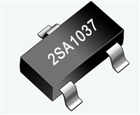
 2SA1037KPT资料详解:产品特性、电气参数、设计指南
