
 5秒后页面跳转

| 型号 | 品牌 | 替代类型 | 描述 | 数据表 |
| AD7228ACR | ADI |
完全替代  |
LC2MOS Octal 8-Bit DAC |

|
| AD7228ABR | ADI |
完全替代 |
LC2MOS Octal 8-Bit DAC |
|
| 型号 | 品牌 | 获取价格 | 描述 | 数据表 |
| AD7228ABRZ-REEL | ADI |
获取价格 |
LC2MOS Octal 8-Bit DAC |
|
| AD7228ACN | ADI |
获取价格 |
LC2MOS Octal 8-Bit DAC |
|
| AD7228ACP | ADI |
获取价格 |
LC2MOS Octal 8-Bit DAC |
|
| AD7228ACPZ-REEL | ADI |
获取价格 |
LC2MOS Octal 8-Bit DAC |
|
| AD7228ACQ | ADI |
获取价格 |
LC2MOS Octal 8-Bit DAC |
|
| AD7228ACR | ADI |
获取价格 |
LC2MOS Octal 8-Bit DAC |
|
| AD7228ATQ | ADI |
获取价格 |
LC2MOS Octal 8-Bit DAC Mount Packages |
|
| AD7228ATQ/883B | ETC |
获取价格 |
8-Bit Digital-to-Analog Converter |
|
| AD7228ATQ3 | ADI |
获取价格 |
LC2MOS Octal 8-Bit DAC |
|
| AD7228AUQ | ADI |
获取价格 |
LC2MOS Octal 8-Bit DAC |
|
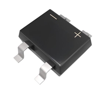 数据手册解读:MB10S引脚说明、电气参数

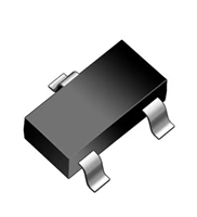 2N7002K资料解读:产品特性和型号推荐
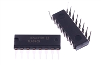 资料解读:TL494CN参数和引脚功能图说明
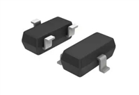 解读BAT54A数据手册:全面解析产品特性与应用
工作时间:9:00-21:00
CEO邮箱:ceo@jiepei.com
投诉邮箱:tousu@jiepei.com


 浙公网安备 33010502006866号 浙ICP备10014259号-119
营业执照ICP证
浙公网安备 33010502006866号 浙ICP备10014259号-119
营业执照ICP证


