AD660
AD660AN/AR/SQ
AD660BN/BR
Parameter
POWER SUPPLIES
Voltage
Min
Typ
Max
Min
Typ
Max
Unit
6
+VCC
+13.5
−13.5
+4.5
+16.5
−16.5
+5.5
+13.5
−13.5
+4.5
+16.5
−16.5
+5.5
V
V
V
6
−VEE
+VLL
Current (No Load)
ICC
IEE
ILL
+12
−12
+18
−18
+12
−12
+18
−18
mA
mA
@ VIH = 5 V, VIL = 0 V
@ VIH = 2.4 V, VIL = 0.4 V
Power Supply Sensitivity
Power Dissipation (Static, No Load)
TEMPERATURE RANGE
0.3
3
1
2
7.5
2
0.3
3
1
2
7.5
2
mA
mA
ppm/%
mW
365
625
365
625
Specified Performance (A, B)
Specified Performance (S)
−40
−55
+85
+125
−40
+85
°C
°C
1 For 16-bit resolution, 1 LSB = 0.0015% of FSR. For 15-bit resolution, 1 LSB = 0.003% of FSR. For 14-bit resolution, 1 LSB = 0.006% of FSR. FSR stands for full-scale range
and is 10 V in a unipolar mode and 20 V in bipolar mode.
2 Gain error and gain drift are measured using the internal reference. The internal reference is the main contributor to gain drift. If lower gain drift is required, the AD660
can be used with a precision external reference such as the AD587, AD586, or AD688.
3 Gain error is measured with fixed 50 Ω resistors as shown in the Theory of Operation section. Eliminating these resistors increases the gain error by 0.25% of FSR
(unipolar mode) or 0.50% of FSR (bipolar mode).
4 DAC gain error and drift are measured with an external voltage reference. They represent the error contributed by the DAC alone, for use with an external reference.
5 External current is defined as the current available in addition to that supplied to REF IN and SPAN/BIPOLAR OFFSET on the AD660.
6 Operation on 12 V supplies is possible using an external reference such as the AD586 and reducing the output range. Refer to the Internal/External Reference Use
section.
AC PERFORMANCE CHARACTERISTICS
With the exception of total harmonic distortion + noise (THD + N) and signal-to-noise (SNR) ratio, these characteristics are included for
design guidance only and are not subject to test. THD + N and SNR are 100% tested.
TMIN ≤ TA ≤ TMAX, +VCC = 15 V, −VEE = −15 V, +VLL = 5 V except where noted.
Table 2.
Parameter
ꢀimit
13
8
10
6
Unit
Test Conditions/Comments
20 V step, TA = 25°C
20 V step, TA = 25°C
20 V step, TMIN ≤ TA ≤ TMAX
10 V step, TA = 25°C
10 V step, TMIN ≤ TA ≤ TMAX
1 LSB step, TMIN ≤ TA ≤ TMAX
OUTPUT SETTLING TIME
(Time to 0.0008% FS
with 2 kΩ, 1000 pF Load)
μs max
μs typ
μs typ
μs typ
μs typ
μs typ
8
2.5
TOTAL HARMONIC DISTORTION + NOISE
A, B, S Grade
A, B, S Grade
0.009
0.056
5.6
% max
% max
% max
dB min
nV-s typ
nV-s typ
0 dB, 990.5 Hz, sample rate = 96 kHz, TA = 25°C
−20 dB, 990.5 Hz, sample rate = 96 kHz, TA = 25°C
−60 dB, 990.5 Hz, sample rate = 96 kHz, TA = 25°C
TA = 25°C
A, B, S Grade
SIGNAL-TO-NOISE RATIO
DIGITAL-TO-ANALOG GLITCH IMPULSE
DIGITAL FEEDTHROUGH
83
15
DAC alternately loaded with 0x8000 and 0x7FFF
DAC alternately loaded with 0x0000 and 0xFFFF, CS high
2
OUTPUT NOISE VOLTAGE
Density (1 kHz to 1 MHz)
REFERENCE NOISE
120
125
nV/√Hz typ
nV/√Hz typ
Measured at VOUT, 20 V span, excludes reference
Measured at REF OUT
Rev. B | Page 4 of 20


 深入解析AD7606高性能多通道模数转换器:资料手册参数分析

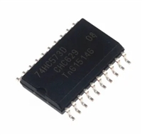
 74HC573三态非易失锁存器(Latch)资料手册参数分析

 MAX3232 RS-232电平转换器资料手册参数分析

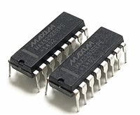
 MAX485 RS-485/RS-422收发器资料手册参数分析
