AD640
(V = ؎5 V, T = +25؇C, unless otherwise noted)
AC SPECIFICATIONS
S
A
Model
AD640J
Typ
AD640B
Typ
AD640T
Typ
Parameter
Conditions
Min
Max
Min
Max
Min
Max
Units
SIGNAL INPUTS (Pins 1, 20)
Input Capacitance
Noise Spectral Density
Tangential Sensitivity
Either Pin to COM
1 kHz to 10 MHz
BW = 100 MHz
2
2
–72
2
2
–72
2
2
–72
pF
nV/√Hz
dBm
3 dB BANDWIDTH
Each Stage
All Five Stages
350
145
350
145
350
145
MHz
MHz
Pins 1 & 20 to 10 & 11
LOGARITHMIC OUTPUTS5
Slope Current, IY
f< = 1 MHz
0.96
0.88
0.82
1.0
1.04
1.00
0.98
0.98
0.91
0.86
1.0
1.02
0.97
0.94
0.98
0.91
0.86
1.0
1.02
0.97
0.94
mA
mA
mA
mA
mA
f = 30 MHz
f = 60 MHz
f = 90 MHz
f = 120 MHz
0.94
0.90
0.88
0.85
0.94
0.90
0.88
0.85
0.94
0.90
0.88
0.85
Intercept, Dual AD640s10, 11
f< = 1 MHz
–90.6 –88.6 –86.6
–89.6
–88.6
–87.6
–86.3
–83.9
–80.3
–87.6
–89.6
–88.6 –87.6
–87.6
–86.3
–83.9
–80.3
dBm
dBm
dBm
dBm
dBm
f = 30 MHz
f = 60 MHz
f = 90 MHz
f = 120 MHz
–87.6
–86.3
–83.9
–80.3
AC LINEARITY
–40 dBm to –2 dBm12
–35 dBm to –10 dBm12
–75 dBm to 0 dBm10
–70 dBm to –10 dBm10
–75 dBm to +15 dBm13
f = 1 MHz
f = 1 MHz
f = 1 MHz
f = 1 MHz
f = 10 kHz
0.5
2.0
1.0
3.0
2.0
3.0
0.5
1.0
0.5
1.5
1.0
1.5
0.5
1.0
0.5
1.5
1.0
1.5
dB
dB
dB
dB
dB
0.25
0.75
0.5
0.25
0.75
0.5
0.25
0.75
0.5
0.5
0.5
0.5
PACKAGE OPTION
20-Lead Ceramic DIP Package (D)
20-Terminal Ceramic LCC (E)
20-Lead Plastic DIP Package (N)
20-Lead Plastic Leaded Chip Carrier (P)
AD640BD
AD640BE
AD640TD
AD640TE
AD640]N
AD640JP
AD640BP
155
NUMBER OF TRANSISTORS
NOTES
155
155
1Logarithms to base 10 are used throughout. The response is independent of the sign of V IN
.
2Attenuation ratio trimmed to calibrate intercept to 10 mV when in use. It has a temperature coefficient of +0.30%/ °C.
3Overall gain is trimmed using a ± 200 µV square wave at 2 kHz, corrected for the onset of compression.
4The fully limited signal output will appear to be a square wave; its amplitude is proportional to absolute temperature.
5Currents defined as flowing into Pin 14. See FUNDAMENTALS OF LOGARITHMIC CONVERSION for full explanation of scaling concepts. Slope is measured
by linear regression over central region of transfer function.
6The logarithmic intercept in dBV (decibels relative to 1 V) is defined as 20 LOG10 (VX/1 V).
7The zero-signal current is a function of temperature unless internal temperature compensation (ITC) pin is grounded.
8Operating in circuit of Figure 24 using ± 0.1% accurate values for RLA and RLB. Includes slope and nonlinearity errors. Input offset errors also included for
VIN >3 mV dc, and over the full input range in ac applications.
9Essentially independent of supply voltages.
10Using the circuit of Figure 27, using cascaded AD640s and offset nulling. Input is sinusoidal, 0 dBm in 50 Ω = 223 mV rms.
11For a sinusoidal signal (see EFFECT OF WAVEFORM ON INTERCEPT). Pin 8 on second AD640 must be grounded to ensure temperature stability of intercept
for dual AD640 system.
12Using the circuit of Figure 24, using single AD640 and offset nulling. Input is sinusoidal, 0 dBm in 50 Ω = 223 mV rms.
13Using the circuit of Figure 32, using cascaded AD640s and attenuator. Square wave input.
All min and max specifications are guaranteed, but only those in boldface are 100% tested on all production units. Results from those tests are used to calculate
outgoing quality levels.
Specifications subject to change without notice.
THERMAL CHARACTERISTICS
JC (؇C/W)
JA (؇C/W)
20-Lead Ceramic DIP Package (D-20)
20-Terminal Ceramic LCC (E-20A)
20-Lead Plastic DIP Package (N-20)
20-Lead Plastic Leaded Chip Carrier (P-20A)
25
25
24
28
85
85
61
75
REV. C
–3–


 MAX3232 RS-232电平转换器资料手册参数分析

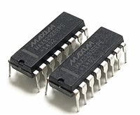
 MAX485 RS-485/RS-422收发器资料手册参数分析

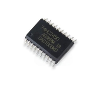
 74HC245八路双向总线收发器:资料手册参数分析

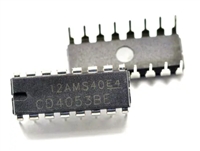
 CD4053模拟多路复用器/解复用器:资料手册参数分析
