AD586
THEORY OF OPERATION
V
IN
IN
The AD586 consists of a proprietary buried Zener diode refer-
ence, an amplifier to buffer the output, and several high stability
thin-film resistors, as shown in the block diagram in Figure 5.
This design results in a high precision monolithic 5 V output
reference with initial offset of 2.0 mV or less. The temperature
compensation circuitry provides the device with a temperature
coefficient of under 2 ppm/°C.
2
V
6
5
V
OUTPUT
O
AD586
NOISE
REDUCTION
8
10kΩ
TRIM
OPTIONAL
NOISE
REDUCTION
CAPACITOR
C
1µF
N
GND
4
Using the bias compensation resistor between the Zener output
and the noninverting input to the amplifier, a capacitor can be
added at the noise reduction pin (Pin 8) to form a low-pass
filter and reduce the noise contribution of the Zener to the
circuit.
Figure 6. Optional Fine-Trim Configuration
NOISE PERFORMANCE AND REDUCTION
The noise generated by the AD586 is typically less than 4 µV p-p
over the 0.1 Hz to 10 Hz band. Noise in a 1 MHz bandwidth is
approximately 200 µV p-p. The dominant source of this noise is
the buried Zener, which contributes approximately 100 nV/√Hz.
By comparison, contribution by the op amp is negligible. Figure 7
shows the 0.1 Hz to 10 Hz noise of a typical AD586. The noise
measurement is made with a band-pass filter made of a 1-pole
high-pass filter with a corner frequency at 0.1 Hz, and a 2-pole
low-pass filter with a corner frequency at 12.6 Hz, to create a
filter with a 9.922 Hz bandwidth.
V
IN
NOISE REDUCTION
8
2
AD586
R
Z1
R
S
A1
6
5
V
OUT
R
Z2
R
F
R
T
TRIM
R
I
If further noise reduction is desired, an external capacitor can
be added between the noise reduction pin and ground, as
shown in Figure 6. This capacitor, combined with the 4 kΩ RS
and the Zener resistances, forms a low-pass filter on the output
of the Zener cell. A 1 µF capacitor will have a 3 dB point at
12 Hz, and will reduce the high frequency (to 1 MHz) noise to
about 160 µV p-p. Figure 8 shows the 1 MHz noise of a typical
AD586, both with and without a 1 µF capacitor.
4
GND
NOTES
1. PINS 1, 3, AND 7 ARE INTERNAL TEST POINTS.
MAKE NO CONNECTIONS TO THESE POINTS.
Figure 5. Functional Block Diagram
APPLYING THE AD586
The AD586 is simple to use in virtually all precision reference
applications. When power is applied to Pin 2 and Pin 4 is
grounded, Pin 6 provides a 5 V output. No external components
are required; the degree of desired absolute accuracy is achieved
simply by selecting the required device grade. The AD586
requires less than 3 mA quiescent current from an operating
supply of 12 V or 15 V.
1µF
5s
1µF
An external fine trim may be desired to set the output level to
exactly 5.000 V (calibrated to a main system reference). System
calibration may also require a reference voltage that is slightly
different from 5.000 V, for example, 5.12 V for binary applica-
tions. In either case, the optional trim circuit shown in Figure 6
can offset the output by as much as 300 mV with minimal effect
on other device characteristics.
Figure 7. 0.1 Hz to 10 Hz Noise
Rev. G | Page 7 of 16


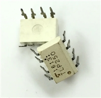
 TLP250光耦合器:资料手册参数分析

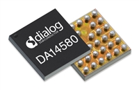
 DA14580 低功耗蓝牙系统级芯片(SoC):资料手册参数分析

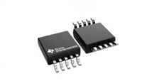
 INA226 高精度电流和功率监控器:资料手册参数分析

 SI2302 N沟道MOSFET:资料手册参数分析
