PRELIMINARY TECHNICAL DATA
Nonvolatile Memory Digital Potentiometers AD5231/AD5232/AD5233
SERIAL DATA INTERFACE
OPERATIONAL OVERVIEW
The AD523X family contains a four-wire SPI compatible digital
interface (SDI, SDO, CS, and CLK). Key features of this
interface include:
The AD5231/32/33 digital potentiometer family is designed to
operate as a true variable resistor replacement device for analog
signals that remain within the terminal voltage range of
VSS<VTERM<VDD. The basic voltage range is limited to a |VDD
VSS| < 5.5V.
-
•
•
Independently Programmable Read & Write to all registers
Direct parallel refresh of all RDAC wiper registers from
corresponding internal EEMEM registers
Increment & Decrement instructions for each RDAC wiper
register
Left & right Bit Shift of all RDAC wiper registers to
achieve 6dB level changes
Nonvolatile storage of the present scratch pad RDAC
register values into the corresponding EEMEM register
Extra bytes of user addressable electrical-erasable memory
Control of the digital potentiometer allows both scratch pad
register (RDAC register) changes to be made, as well as,
100,000 nonvolatile electrically erasable memory (EEMEM)
register operations. The EEMEM update process takes
approximately 20.2ms, during this time the shift register is
locked preventing any changes from taking place. The RDY pin
flags the completion of this EEMEM save. The EEMEM
retention is designed to last 15 years at 85°C, which is
equivalent to 90 years at 55°C, without refresh.
•
•
•
•
The serial interface contains three different word formats to
support the single AD5231, dual AD5232, and the quad
AD5233 digital potentiometer devices. The AD5232 and
AD5233 use a 16-bit serial data word loaded MSB first, while
the AD5231 uses a 24-bit serial word loaded MSB first. The
format of the SPI compatible word is shown in Table 1 and 2.
The Command Bits (Cx) control the operation of the digital
potentiometer according to the command instructions shown in
Table 3, 4, and 5. The Address Bits (Ax) determine which
register is activated. The Data Bits (Dx) are the values that are
loaded into the decoded register. The last instruction executed
prior to a period of no programming activity should be the No
OPeration (NOP) instruction. This will place the internal logic
circuitry in a minimum power dissipation state.
The scratch pad register can be changed incrementally by using
the software controlled Increment/Decrement instruction or the
Shift Left/Right instruction command. Once an Increment,
Decrement or Shift command has been loaded into the shift
register subsequent CS strobes will repeat this command. This is
useful for push button control applications. Alternately the
scratch pad register can be programmed with any position value
using the standard SPI serial interface mode by loading the
representative data word. The scratch pad register can be loaded
with the current contents of the nonvolatile EEMEM register
under program control. At system power ON, the default value
of the scratch pad memory is the value previously saved in the
EEMEM register. The factory EEMEM preset value is midscale.
The scratch pad (wiper) register can be loaded with the current
contents of the nonvolatile EEMEM register under hardware
control by pulsing the PR pin. Beware that the PR pulse first sets
the wiper at midscale when brought to logic zero, and then on
the positive transition to logic high, it reloads the DAC wiper
register with the contents of EEMEM. Similarly, the saved
EEMEM value will automatically be retrieved to the scratch pad
register during system power ON.
PR
VALID
COMMAND
COMMAND
+5V
PROCESSOR
& ADDRESS
DECODE
COUNTER
R PULLUP
CLK
SERIAL
REGISTER
A serial data output pin is available for daisy chaining and for
readout of the internal register contents. The serial input data
register uses a 16 or 24-bit instruction/address/data WORD.
Write protect (WP) disables any changes of current content in
the scratch pad register regardless of the commands, except that
EEMEM setting can be retrieved using commands 1 and 9.
Therefore, write-protect (WP) pin provides hardware EEMEM
protection feature.
SDO
GND
CS
SDI
Figure 2. Equivalent Digital Input-Output Logic
The equivalent serial data input and output logic is shown in
figure 2. The open drain output SDO is disabled whenever chip
select CS is logic high. The SPI interface can be used in two
slave modes CPHA=1, CPOL=1 and CPHA=0, CPOL=0. CPHA
and CPOL refer to the control bits, which dictate SPI timing in
the following microprocessors/Micro Converters:
DIGITAL INPUT/OUTPUT CONFIGURATION
All digital inputs are ESD protected high input impedance that
can be driven directly from most digital sources. For PR and WP,
which are active at logic low, can be tied directly to VDD if they
are not being used.
ADuC812/824, M68HC11, and MC68HC16R1/916R1.
The SDO and RDY pins are open drain digital outputs where
pull-up resistors are needed only if using these functions. A
resistor value in the range of 1k to 10k ohm optimizes the power
and switching speed trade off.
REV PrF
7
22 MAR '01
Information contained in this Preliminary data sheet describes a product in the early definition stage. There is no guarantee that the
information contained here will become a final product in its present form. For latest information contact Walt Heinzer/Analog Devices, Santa
Clara, CA. TEL(408)382-3107; FAX (408)382-2708; walt.heinzer@analog.com


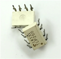
 TLP250光耦合器:资料手册参数分析

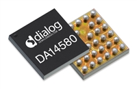
 DA14580 低功耗蓝牙系统级芯片(SoC):资料手册参数分析

 INA226 高精度电流和功率监控器:资料手册参数分析

 SI2302 N沟道MOSFET:资料手册参数分析
