AD1864
ABSOLUTE MAXIMUM RATINGS*
VL to DGND . . . . . . . . . . . . . . . . . . . . . . . . . . . 0 V to 13.2 V
VS to AGND . . . . . . . . . . . . . . . . . . . . . . . . . . . 0 V to 13.2 V
–VL to DGND . . . . . . . . . . . . . . . . . . . . . . . . . –13.2 V to 0 V
–VS to AGND . . . . . . . . . . . . . . . . . . . . . . . . . –13.2 V to 0 V
AGND to DGND . . . . . . . . . . . . . . . . . . . . . . . . . . . . +0.3 V
Digital Inputs to DGND . . . . . . . . . . . . . . . . . . . –0.3 V to VL
Short-Circuit Protection . . . . . . . . Indefinite Short to Ground
Soldering (10 sec) . . . . . . . . . . . . . . . . . . . . . . . . . . . .+300°C
*Stresses greater than those listed under Absolute Maximum Ratings may cause
permanent damage to the device. This is a stress rating only; functional operation
of the device at these or any other conditions above those indicated in the
operational section of this specification is not implied. Exposure to absolute
maximum rating conditions for extended periods may affect device reliability.
CAUTION
ESD (electrostatic discharge) sensitive device. Electrostatic charges as high as 4000 V readily
accumulate on the human body and test equipment and can discharge without detection.
Although the AD1864 features proprietary ESD protection circuitry, permanent damage may
occur on devices subjected to high energy electrostatic discharges. Therefore, proper ESD
precautions are recommended to avoid performance degradation or loss of functionality.
WARNING!
ESD SENSITIVE DEVICE
PIN FUNCTION DESCRIPTIONS
Description
PIN CONFIGURATIONS
DIP Package
Signal
–VS
Negative Analog Supply
24
+VS
1
2
–VS
TRIM
MSB
IOUT
AGND
SJ
Right Channel Trim Network Connection
Right Channel Trim Potentiometer Connection
Right Channel Output Current
Right Channel Analog Common Pin
Right Channel Amplifier Summing Junction
Right Channel Feedback Resistor
Right Channel Output Voltage
Positive Digital Supply
Right Channel Data Input Pin
Right Channel Latch Pin
Clock Input Pin
Digital Common Pin
Left Channel Latch Pin
TRIM
23 TRIM
22
21
20
19
18
17
16
15
14
13
3
MSB
I OUT
AGND
SJ
MSB
I OUT
AGND
SJ
RIGHT
CHANNEL
LEFT
CHANNEL
4
RF
5
VOUT
+VL
DR
AD1864
6
TOP VIEW
(Not to Scale)
RF
7
RF
LR
8
VOUT
–V L
DL
VOUT
+VL
CLK
DGND
LL
DL
–VL
9
10
DR
Left Channel Data Input Pin
Negative Digital Supply
LR 11
12
LL
CLK
DGND
VOUT
RF
SJ
AGND
IOUT
MSB
TRIM
+VS
Left Channel Output Voltage
Left Channel Feedback Resistor
Left Channel Amplifier Summing Junction
Left Channel Analog Common Pin
Left Channel Output Current
Left Channel Trim Potentiometer Wiper Connection
Left Channel Trim Network Connection
Positive Analog Supply
PLCC Package
28 27 26
3
2
1
4
I
25
5
I
OUT
OUT
AGND
6
7
24
23
22
AGND
SJ
ORDERING GUIDE
SJ
NC
RF
AD1864
THD+N
@ Full Scale
Package
Option*
8
NC
TOP VIEW
(Not to Scale)
Model
9
21 RF
V
10
11
AD1864N
0.006%
0.004%
0.0025%
0.006%
0.004%
N-24
N-24
N-24
P-28A
P-28A
20
V
OUT
OUT
AD 1864N-J
AD1864N-K
AD1864P
19 –V
+V
L
L
12 13
17 18
14 15 16
AD1864P-J
*N = Plastic DIP; P = Plastic Leaded Chip Carrier.
NC = NO CONNECT
REV. A
–4–


 SI2301 N沟道MOSFET:资料手册参数分析

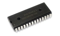
 ADC0809逐次逼近寄存器型模数转换器:资料手册参数分析

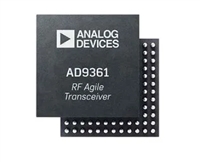
 AD9361捷变收发器:全面参数解析与关键特性概览

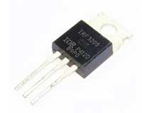
 IRF3205功率MOSFET:资料手册参数分析
