AD1819B
PRODUCT OVERVIEW
Each channel of the ADC is independent, and can process
left and right channel data at different sample rates. All pro-
grammed sample rates from 7 kHz to 48 kHz have a resolution
of 1 Hz. The AD1819B also supports irrational V.34 sample
rates.
The AD1819B SoundPort Codec is designed to meet all require-
ments of the Audio Codec ’97, Component Specification, Revision
1.03, © 1996, Intel Corporation, found at www.Intel.com. In
addition, the AD1819B supports multiple codec configurations
(up to three per AC-Link), a DSP serial mode, variable sample
rates, modem sample rates and filtering, and built-in Phat Ste-
reo 3D enhancement.
Sample Rates and D2S
The AD1819B default mode sets the codec to operate at 48 kHz
sample rates. The converter pairs may process left and right
channel data at different sample rates. The AD1819B sample
rate generator allows the codec to instantaneously change and
process sample rates from 7 kHz to 48 kHz with a resolution of
1 Hz. The in-band integrated noise and distortion artifacts in-
troduced by rate conversions are below –90 dB. The AD1819B
uses a 4-bit D/A structure and Data Directed Scrambling (D2S)
to enhance noise immunity on motherboards and in PC enclo-
sures, and to suppress idle tones below the device’s quantization
noise floor. The D2S process pushes noise and distortion arti-
facts caused by errors in the multibit D/A conversion process to
frequencies beyond the audible range of the human ear and then
filters them.
The AD1819B is an analog front end for high performance PC
audio, modem, or DSP applications. The AC’97 architecture
defines a 2-chip audio solution comprising a digital audio con-
troller, plus a high quality analog component that includes
Digital-to-Analog Converters (DACs), Analog-to-Digital Con-
verters (ADCs) mixer and I/O.
The main architectural features of the AD1819B are the high
quality analog mixer section, two channels of Σ∆ ADC conver-
sion, two channels of Σ∆ DAC conversion and Data Direct
Scrambling (D2S) rate generators. The AD1819B’s left channel
ADC and DAC are compatible for modem applications support-
ing irrational sample rates and modem filtering requirements.
Digital-to-Analog Signal Path
FUNCTIONAL DESCRIPTION
The analog output of the DAC may be gained or attenuated
from +12 dB to –34.5 dB in 1.5 dB steps, and summed with any
of the analog input signals. The summed analog signal enters
the Master Volume stage where each channel of the mixer out-
put may be attenuated from 0 dB to –46.5 dB in 1.5 dB steps or
muted.
This section overviews the functionality of the AD1819B and is
intended as a general introduction to the capabilities of the
device. Detailed reference information may be found in the
descriptions of the Indexed Control Registers.
Analog Inputs
The codec contains a stereo pair of Σ∆ ADCs. Inputs to the
ADC may be selected from the following analog signals: tele-
phony (PHONE_IN), mono microphone (MIC1 or MIC2),
stereo line (LINE_IN), auxiliary line input (AUX), stereo CD
ROM (CD), stereo audio from a video source (VIDEO) and
post-mixed stereo or mono line output (LINE_OUT).
Host-Based Echo Cancellation Support
The AD1819B supports time correlated I/O data format by
presenting mic data on the left channel of the ADC and the
mono summation of left and right output on the right channel.
The ADC is splittable; left and right ADC data can be sampled
at different rates.
Analog Mixing
Telephony Modem Support
PHONE_IN, MIC1 or MIC2, LINE_IN, AUX, CD and
VIDEO can be mixed in the analog domain with the stereo
output from the DACs. Each channel of the stereo analog in-
puts may be independently gained or attenuated from +12 dB
to –34.5 dB in 1.5 dB steps. The summing path for the mono
inputs (PHONE_IN, MIC1, and MIC2 to LINE_OUT) dupli-
cates mono channel data on both the left and right LINE_OUT.
Additionally, the PC attention signal (PC_BEEP) may be
mixed with the line output. A switch allows the output of the
DACs to bypass the Phat Stereo 3D enhancement.
The AD1819B contains a V.34-capable analog front end for
supporting host-based and data pump modems. The modem
DAC typical dynamic range is 90 dB over a 4.2 kHz analog
output passband where FS = 12.8 kHz. The left channel of the
ADC and DAC may be used to convert modem data at the same
sample rate in the range between 7 kHz and 48 kHz. All pro-
grammed sample rates have a resolution of 1 Hz. The AD1819B
supports irrational V.34 sample rates with 8/7 and 10/7 select-
able sample rate multiplier coefficients.
Differences Between the AD1819A and AD1819B
The voltage reference (VREF) of the AD1819B remains active
while RESET is asserted. This eliminates the audible artifacts
associated with the RESET LO to HI transitions that can
occur during a Windows boot (power-up) or Windows warm
restart (reset).
Analog-to-Digital Signal Path
The selector sends left and right channel signals to the program-
mable gain amplifier (PGA). The PGA following the selector
allows independent gain for each channel entering the ADC
from 0 dB to +22.5 dB in 1.5 dB steps.
REV. 0
–2–


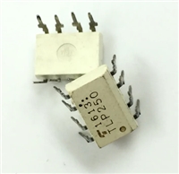
 TLP250光耦合器:资料手册参数分析

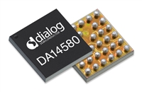
 DA14580 低功耗蓝牙系统级芯片(SoC):资料手册参数分析

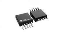
 INA226 高精度电流和功率监控器:资料手册参数分析

 SI2302 N沟道MOSFET:资料手册参数分析
