Wide Input Voltage, 2.4 MHz, 3.0 AAsynchronous Buck Regulator With
Low-IQ Standby, Sleep Mode, External Synchronization, and NPOR Output
A8590
ELECTRICAL CHARACTERISTICS (continued): valid at 4.0 V ≤ VIN ≤ 35 V; –40ºC ≤ TA = TJ ≤ 150ºC; unless otherwise
specified.
Characteristics
Error Amplifier
Symbol
Test Conditions
Min.
Typ.
Max.
Unit
Feedback Input Bias Current7
Open Loop Voltage Gain
IFB
–38
–
–
–16
–
nA
dB
AVOL
VCOMP = 1.2 V
400 mV < VFB
65
500
275
–
750
375
±75
1
950
475
–
µA/V
µA/V
µA
Transconductance
gm
0 V < VFB < 400 mV
VCOMP = 1.2 V
Output Current
IEA
COMP Pull-Down Resistance
Pulse Width Modulation (PWM)
PWM Ramp Offset
RCOMP
FAULT = 1 or HICCUP = 1
–
–
kΩ
PWMOFFS
VCOMP level required for 0% duty cycle
–
–
400
95
–
mV
ns
12 V < VIN < 16 V, IOUT = 1 A, VBOOT – VSW
4.5 V
=
Minimum Controllable PWM On-Time
tON(MIN)PWM
135
Minimum Switch Off-Time
COMP to SW Current Gain
tOFF(MIN)PWM
gmPOWER
–
95
130
–
ns
–
4.0
A/V
fOSC = 2.44 MHz
2.31
0.66
0.15
3.30
1.00
0.22
4.30
1.32
0.29
A/µs
A/µs
A/µs
Slope Compensation8
SE
f
OSC = 1.00 MHz
OSC = 252 kHz
f
MOSFET Parameters6
TJ =25ºC, VBOOT – VSW = 4.5 V, IDS = 0.4 A
TJ =150ºC, VBOOT – VSW = 4.5 V, IDS = 0.4 A
–
–
110
190
125
215
mΩ
mΩ
High-Side MOSFET On-Resistance9
RDS(on)HS
TJ < 85°C, VSLEEP ≤ 0.5 V, VSW = 0 V, VIN
16 V
=
–
–
–
10
µA
µA
High-Side MOSFET Leakage7,10
Ilkg(HS)
TJ ≤ 150°C, VSLEEP ≤ 0.5 V, VSW = 0 V, VIN
16 V
=
60
150
SW Node Slew Rate8
SRSW
12 V < VIN < 16 V
–
–
0.72
–
–
V/ns
Low-Side MOSFET On-Resistance9
PWM Switching Frequency
RDS(on)LS
TJ = 25ºC, VIN ≥ 6 V, IDS = 0.1 A
10
Ω
RFSET = 8.06 kΩ, VPWM/PFM = high
RFSET = 23.7 kΩ, VPWM/PFM = high
RFSET = 102 kΩ, VPWM/PFM = high
2.20
0.90
–
2.44
1.00
252
2.70
1.10
–
MHz
MHz
kHz
Base PWM Switching Frequency
fOSC
PWM Synchronization Timing
1.2 ×
fOSC(typ)
1.5 ×
fOSC(typ)
Synchronization Frequency Range
fSYNC(MULT)
–
–
Synchronized PWM Frequency
Synchronization Input Duty Cycle
Synchronization Input Pulse Width
Synchronization Input Rise Time8
Synchronization Input Fall Time8
fSYNC(PWM)
DSYNC
twSYNC
trSYNC
–
–
–
–
2.9
80
–
MHz
%
200
–
–
ns
10
10
15
15
ns
tfSYNC
–
ns
Continued on next page...
6Thermally limited depending on input voltage, output voltage, duty cycle, regulator load currents, PCB layout, and airflow.
7Negative current is defined as coming out of the node or pin, positive current is defined as going into the node or pin.
8Ensured by design and characterization, not production tested.
9Performance at 25°C ensured by design and characterization, not production tested.
10Performance at 85°C ensured by design and characterization, not production tested.
Allegro MicroSystems, LLC
115 Northeast Cutoff
7
Worcester, Massachusetts 01615-0036 U.S.A.
1.508.853.5000; www.allegromicro.com


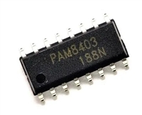
 PAM8403音频功率放大器:资料手册参数分析

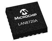
 LAN8720以太网收发器:资料手册参数分析

 SI2301 N沟道MOSFET:资料手册参数分析

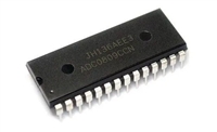
 ADC0809逐次逼近寄存器型模数转换器:资料手册参数分析
