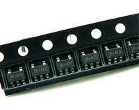
Wide Input Voltage Range, High-Efficiency,
Fault-Tolerant LED Driver
A8518 and A8518-1
PINOUT DIAGRAM AND TERMINAL LIST TABLE
16 LED2
15 LED1
14 AGND
13 ISET
12 APWM
11 PWM
10 VDD
COMP
PGND
OVP
1
2
3
4
5
6
7
8
VOUT
SW
PAD
GATE
VSENSE
VIN
9
FAULT
Package LP, 16-Pin TSSOP Pinout Diagram
Terminal List Table
Name
Number
Function
Output of the error amplifier and compensation node. Connect a series RZ-CZ-CP network from this pin to GND for control
loop compensation.
1
COMP
2
3
PGND
OVP
Power ground for internal N-channel MOSFET switching device.
Overvoltage protection. Connect external resistor from VOUT to this pin to adjust the overvoltage protection level.
4
5
6
VOUT
SW
Connect directly to boost output voltage.
The drain of the internal N-channel MOSFET switching device of the boost converter.
Output gate driver pin for external P-channel MOSFET control.
GATE
Connect this pin to the negative sense side of the current sense resistor RSC. The threshold voltage is measured as VIN-
VSENSE. There is also fixed current sink to allow for trip threshold adjustment.
7
8
VSENSE
VIN
Input power to the IC, as well as the positive input used for current sense resistor.
The pin is an open-drain type configuration that will be pulled low when a fault occurs. Connect a 100 kΩ resistor between
this pin and desired logic level voltage.
9
FAULT
VDD
10
11
Output of internal LDO (bias regulator). Connect a 1 µF decoupling capacitor between this pin and GND.
Enables the IC when this pin is pulled high. Also serves to control the LED intensity by using pulse-width modulation.
Typical PWM dimming frequency is in the range of 100 to 400 Hz.
PWM
12
13
14
APWM
ISET
Analog trimming option or dimming. Applying a digital PWM signal to this pin adjusts the internal ISET current.
Connect RISET resistor between this pin and GND to set the desired LED current setting.
LED current ground. Connect to PCB ground plane.
AGND
LED current sink #1. Connect the cathode of LED string to associated pin. Unused LEDx pin must be terminated to GND
through a 1.54 kΩ resistor.
15
16
–
LED1
LED2
PAD
LED current sink #2. Connect the cathode of LED string to associated pin. Unused LEDx pin must be terminated to GND
through a 1.54 kΩ resistor.
Exposed pad of the package providing enhanced thermal dissipation. This pad must be connected to the ground plane(s)
of the PCB with at least 8 vias, directly in the pad.
Allegro MicroSystems, LLC
115 Northeast Cutoff
5
Worcester, Massachusetts 01615-0036 U.S.A.
1.508.853.5000; www.allegromicro.com


 一文带你解读74HC244资料手册:特性、应用场景、封装方式、引脚配置说明、电气参数、推荐替代型号

 AD623资料手册解读:特性、应用、封装、引脚功能及电气参数

 RT9193资料手册解读:RT9193引脚功能、电气参数、替换型号推荐

 VIPER22A的资料手册解读、引脚参数说明、代换型号推荐
