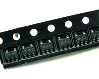
A25L80P Series
SIGNAL DESCRIPTION
Serial Data Output (Q). This output signal is used to transfer
data serially out of the device. Data is shifted out on the
falling edge of Serial Clock (C).
Serial Data Input (D). This input signal is used to transfer
data serially into the device. It receives instructions,
addresses, and the data to be programmed. Values are
latched on the rising edge of Serial Clock (C).
Serial Clock (C). This input signal provides the timing of the
serial interface. Instructions, addresses, or data present at
Serial Data Input (D) are latched on the rising edge of Serial
Clock (C). Data on Serial Data Output (Q) changes after the
falling edge of Serial Clock (C).
Driving Chip Select ( ) Low enables the device, placing it in
S
the active power mode.
After Power-up, a falling edge on Chip Select ( ) is required
S
prior to the start of any instruction.
Hold (
). The Hold (
) signal is used to pause
HOLD
HOLD
any serial communications with the device without
deselecting the device.
During the Hold condition, the Serial Data Output (Q) is high
impedance, and Serial Data Input (D) and Serial Clock (C)
are Don’t Care. To start the Hold condition, the device must
be selected, with Chip Select ( ) driven Low.
S
Chip Select ( ). When this input signal is High, the device
S
Write Protect ( ). The main purpose of this input signal is
W
is deselected and Serial Data Output (Q) is at high
impedance. Unless an internal Program, Erase or Write
Status Register cycle is in progress, the device will be in the
Standby mode (this is not the Deep Power-down mode).
to freeze the size of the area of memory that is protected
against program or erase instructions (as specified by the
values in the BP2, BP1 and BP0 bits of the Status Register).
SPI MODES
the falling edge of Serial Clock (C).
These devices can be driven by a microcontroller with its SPI
peripheral running in either of the two following modes:
– CPOL=0, CPHA=0
– CPOL=1, CPHA=1
For these two modes, input data is latched in on the rising
edge of Serial Clock (C), and output data is available from
The difference between the two modes, as shown in Figure 2,
is the clock polarity when the bus master is in Stand-by mode
and not transferring data:
– C remains at 0 for (CPOL=0, CPHA=0)
– C remains at 1 for (CPOL=1, CPHA=1)
(April, 2007, Version 1.5)
3
AMIC Technology Corp.


 一文带你解读74HC244资料手册:特性、应用场景、封装方式、引脚配置说明、电气参数、推荐替代型号

 AD623资料手册解读:特性、应用、封装、引脚功能及电气参数

 RT9193资料手册解读:RT9193引脚功能、电气参数、替换型号推荐

 VIPER22A的资料手册解读、引脚参数说明、代换型号推荐
