IDT70V7519S
High-Speed 256K x 36 Synchronous Bank-Switchable Dual-Port Static RAM
Industrial and Commercial Temperature Ranges
Truth Table I—Read/Write and Enable Control(1,2,3,4)
Byte 3
I/O27-35
Byte 2
I/O18-26
Byte 1
I/O9-17
Byte 0
I/O0-8
OE3
CLK
↑
↑
↑
↑
↑
↑
↑
↑
↑
↑
↑
↑
↑
↑
↑
↑
↑
X
CE
X
1
R/W
X
X
X
L
MODE
CE
0
BE
3
BE
2
BE
1
BE0
X
H
X
L
L
L
L
L
L
L
L
L
L
L
L
L
L
L
X
X
X
H
H
H
H
L
X
X
H
H
H
L
X
X
H
H
L
X
X
H
L
High-Z
High-Z
High-Z
High-Z
High-Z
High-Z
High-Z
High-Z
High-Z
High-Z
High-Z
High-Z
High-Z
High-Z
High-Z
High-Z Deselected–Power Down
High-Z Deselected–Power Down
High-Z All Bytes Deselected
X
L
X
H
H
H
H
H
H
H
H
H
H
H
H
H
H
H
X
X
DIN
Write to Byte 0 Only
X
H
H
H
L
L
DIN
High-Z Write to Byte 1 Only
High-Z Write to Byte 2 Only
High-Z Write to Byte 3 Only
X
H
H
L
L
DIN
High-Z
High-Z
X
H
H
L
L
DIN
High-Z
High-Z
X
H
L
L
High-Z
DIN
DIN
Write to Lower 2 Bytes Only
X
H
L
H
L
L
DIN
DIN
High-Z
High-Z Write to Upper 2 bytes Only
X
L
L
L
DIN
DIN
DIN
DIN
Write to All Bytes
Read Byte 0 Only
L
H
H
H
L
H
H
L
H
L
L
H
H
H
H
H
H
H
X
High-Z
High-Z
High-Z
High-Z
High-Z
High-Z
DOUT
L
H
H
H
L
DOUT
High-Z Read Byte 1 Only
High-Z Read Byte 2 Only
High-Z Read Byte 3 Only
L
H
H
L
DOUT
High-Z
High-Z
L
H
H
L
DOUT
High-Z
High-Z
L
H
L
High-Z
DOUT
DOUT
Read Lower 2 Bytes Only
High-Z Read Upper 2 Bytes Only
Read All Bytes
High-Z Outputs Disabled
L
H
L
H
L
DOUT
DOUT
High-Z
L
H
L
L
DOUT
DOUT
DOUT
DOUT
X
X
X
X
High-Z
High-Z
High-Z
5618 tbl 02
NOTES:
1. "H" = VIH, "L" = VIL, "X" = Don't Care.
2. ADS, CNTEN, REPEAT are set as appropriate for address access. Refer to Truth Table II for details.
3. OE is an asynchronous input signal.
4. It is possible to read or write any combination of bytes during a given access. A few representative samples have been illustrated here.
Truth Table II—Address and Address Counter Control(1,2,7)
Previous
Address
Addr
Used
Address
CLK
↑
I/O(3)
I/O (n) External Address Used
I/O(n+1) Counter Enabled—Internal Address generation
I/O(n+1) External Address Blocked—Counter disabled (An + 1 reused)
I/O(0) Counter Set to last valid ADS load
MODE
ADS CNTEN REPEAT(6)
An
X
X
An
An
L(4)
H
X
L(5)
H
H
D
An + 1
An + 1
An
D
D
↑
X
An + 1
X
H
H
H
↑
X
X
X
L(4)
D
↑
5618 tbl 03
NOTES:
1. "H" = VIH, "L" = VIL, "X" = Don't Care.
2. Read and write operations are controlled by the appropriate setting of R/W, CE0, CE1, BEn and OE.
3. Outputs configured in flow-through output mode: if outputs are in pipelined mode the data out will be delayed by one cycle.
4. ADS and REPEAT are independent of all other memory control signals including CE0, CE1 and BEn
5. The address counter advances if CNTEN = VIL on the rising edge of CLK, regardless of all other memory control signals including CE0, CE1, BEn.
6. When REPEAT is asserted, the counter will reset to the last valid address loaded via ADS. This value is not set at power-up: a known location should be loaded
via ADS during initialization if desired. Any subsequent ADS access during operations will update the REPEAT address location.
7. The counter includes bank address and internal address. The counter will advance across bank boundaries. For example, if the counter is in Bank 0, at address
FFFh, and is advanced one location, it will move to address 0h in Bank 1. By the same token, the counter at FFFh in Bank 63 will advance to 0h in Bank 0. Refer
to Timing Waveform of Counter Repeat, page 18. Care should be taken during operation to avoid having both counters point to the same bank (i.e., ensure BA0L
- BA5L ≠ BA0R - BA5R), as this condition will invalidate the access for both ports. Please refer to the functional description on page 19 for details.
6.42
6


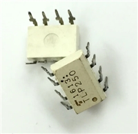
 TLP250光耦合器:资料手册参数分析

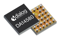
 DA14580 低功耗蓝牙系统级芯片(SoC):资料手册参数分析

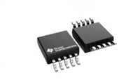
 INA226 高精度电流和功率监控器:资料手册参数分析

 SI2302 N沟道MOSFET:资料手册参数分析
