4.2.1 Additional criteria for device class M.
a. Delete the sequence specified as initial (preburn-in) electrical parameters through interim (postburn-in)
electrical parameters of method 5004 and substitute lines 1 through 6 of table IIA herein.
b. The test circuit shall be maintained by the manufacturer under document revision level control and shall be made
available to the preparing or acquiring activity upon request. The test circuit shall specify the inputs, outputs,
biases, and power dissipation, as applicable, in accordance with the intent specified in test method 1015.
(1) Dynamic burn-in (method 1015 of MIL-STD-883, test condition D; for circuit, see 4.2.1b herein).
c. Interim and final electrical parameters shall be as specified in table IIA herein.
4.2.2 Additional criteria for device classes Q and V.
a. The burn-in test duration, test condition and test temperature, or approved alternatives shall be as specified in the
device manufacturer's QM plan in accordance with MIL-PRF-38535. The burn-in test circuit shall be maintained
under document revision level control of the device manufacturer's Technology Review Board (TRB) in
accordance with MIL-PRF-38535 and shall be made available to the acquiring or preparing activity upon request.
The test circuit shall specify the inputs, outputs, biases, and power dissipation, as applicable, in accordance with
the intent specified in test method 1015 of MIL-STD-883.
b. Interim and final electrical test parameters shall be as specified in table IIA herein.
c. Additional screening for device class V beyond the requirements of device class Q shall be as specified in MIL-
PRF-38535, appendix B.
4.3 Qualification inspection for device classes Q and V. Qualification inspection for device classes Q and V shall be in
accordance with MIL-PRF-38535. Inspections to be performed shall be those specified in MIL-PRF-38535 and herein for
groups A, B, C, D, and E inspections (see 4.4.1 through 4.4.4).
4.4 Conformance inspection. Technology conformance inspection for classes Q and V shall be in accordance with MIL-
PRF-38535 including groups A, B, C, D, and E inspections and as specified herein. Quality conformance inspection for
device class M shall be in accordance with MIL-PRF-38535, appendix A and as specified herein. Inspections to be
performed for device class M shall be those specified in method 5005 of MIL-STD-883 and herein for groups A, B, C, D,
and E inspections (see 4.4.1 through 4.4.4).
4.4.1 Group A inspection.
a. Tests shall be as specified in table IIA herein.
b. Subgroups 5 and 6 of table I of method 5005 of MIL-STD-883 shall be omitted.
c. For device class M, subgroups 7 and 8 tests shall be sufficient to verify the truth table. For device classes Q and
V, subgroups 7 and 8 shall include verifying the functionality of the device.
d. O/V (Latch up) tests shall be measured only for the initial qualification and after any process or design changes
which may affect the performance of the device. For device class M, procedures and circuits shall be manitained
under document revision level control by the manufacturer and shall be made available to the preparing or
acquiring activity upon request. For device classes Q and V, the procedures and circuit shall be under the
control of the device manufacturer’s TRB in accordance with MIL-PRF-38535 and shall be made available to the
preparing or acquiring activity upon request. Testing shall be on all pins, on five devices with zero failures.
Latch-up test shall be considered destructive. Information contained in JEDEC Standard EIA/JESD78 may be
used for reference.
e. Subgroup 4 (CIN and COUT measurements) shall be measured only for initial qualification and after any process or
design changes which may affect input or output capacitance. Capacitance shall be measured between the
designated terminal and GND at a frequency of 1 MHz. Sample size is 15 devices with no failures, and all input
and output terminals tested.
SIZE
STANDARD
5962-93177
MICROCIRCUIT DRAWING
DEFENSE SUPPLY CENTER COLUMBUS
COLUMBUS, OHIO 43216-5000
A
REVISION LEVEL
D
SHEET
6
DSCC FORM 2234
APR 97


 MAX6675资料手册参数详解、引脚配置说明

 LM258引脚图及功能介绍、主要参数分析

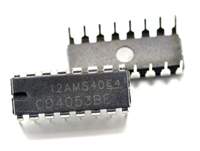
 CD4052资料手册参数详解、引脚配置说明

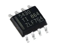
 一文带你了解TPS5430资料手册分析:参数介绍、引脚配置说明
