1.2.3 Device class designator. The device class designator is a single letter identifying the product assurance level as listed
below. Since the device class designator has been added after the original issuance of this drawing, device classes M and Q
designators will not be included in the PIN and will not be marked on the device.
Device class
M
Device requirements documentation
Vendor self-certification to the requirements for MIL-STD-883 compliant,
non-JAN class level B microcircuits in accordance with MIL-PRF-38535,
appendix A
Q or V
Certification and qualification to MIL-PRF-38535
1.2.4 Case outline(s). The case outline(s) are as designated in MIL-STD-1835 and as follows:
Outline letter
Descriptive designator
Terminals
Package style
C
D
E
F
H
P
X
2
GDIP1-T14 or CDIP2-T14
GDFP1-F14 or CDFP2-F14
GDIP1-T16 or CDIP2-T16
GDFP2-F16 or CDFP3-F16
GDFP1-F10 or CDFP2-F10
GDIP1-T8 or CDIP2-T8
CQCC1-N20
14
14
16
16
10
8
Dual-in-line
Flat pack
Dual-in-line
Flat pack
Flat pack
Dual-in-line
Square leadless chip carrier (see figure 1)
Square leadless chip carrier (see figure 1)
20
20
CQCC1-N20
1.2.5 Lead finish. The lead finish is as specified in MIL-PRF-38535 for device classes Q and V or MIL-PRF-38535,
appendix A for device class M.
1.3 Absolute maximum ratings. 1/ 2/ 3/
Supply voltage (V ) .................................................................................. 30 V
CC
Output current ............................................................................................. 1.0 A
Output energy (capacitance load) ............................................................... 5.0 µ j
Analog input voltage (pins 2 and 3) ............................................................ -0.3 V to +6.3 V
Error amplifier output sink current ............................................................... 10 mA
Power dissipation (P )(T = +25°C):
D
A
Cases C, E, F, H, P, X, and 2 .................................................................. 1.0 W 4/
Case D .................................................................................................... 700 mW 4/
Storage temperature range ......................................................................... -65°C to +150°C
Lead temperature (soldering, 10 seconds) ................................................. +300°C
Junction temperature (T ) ........................................................................... +150°C
J
Thermal resistance, junction-to-case (θJC) ................................................ See MIL-STD-1835
1.4 Recommended operating conditions.
Supply voltage (V ) .................................................................................. +15 V 5.0 percent
CC
Ambient operating temperature range (T ) ................................................ -55°C to +125°C
A
1/ Stresses above the absolute maximum rating may cause permanent damage to the device. Extended operation at the
maximum levels may degrade performance and affect reliability.
2/ All voltages are with respect to ground, and all currents are positive when flowing into the specified terminal.
3/ All references to pin numbers are for case outline P.
4/ Derate at 8.0 mW/°C above T = +25°C for case P, 10 mW/°C above T = +50°C for cases C and E,
A
A
5.5 mW/°C above T = +25°C for case D, 8.7 mW/°C above T = +25°C for case F,
A
A
9.0 mW/°C above T = +40°C for cases 2 and X, and 6.9 mW/°C above T = +25°C for case H.
A
A
SIZE
STANDARD
5962-86704
A
MICROCIRCUIT DRAWING
DEFENSE SUPPLY CENTER COLUMBUS
COLUMBUS, OHIO 43216-5000
REVISION LEVEL
SHEET
K
3
DSCC FORM 2234
APR 97


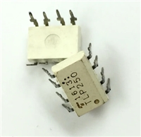
 TLP250光耦合器:资料手册参数分析

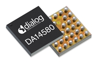
 DA14580 低功耗蓝牙系统级芯片(SoC):资料手册参数分析

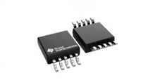
 INA226 高精度电流和功率监控器:资料手册参数分析

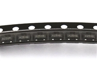
 SI2302 N沟道MOSFET:资料手册参数分析
