Si501/2/3/4
LVCMOS CMEMS® Programmable Oscillator Series
6. The Si502 OE pin has three (3) states: OE High = Freq 1; OE Weak High = Freq 2; OE Low is configurable.
Selected Electrical Specifications
VDD = +1.71 V to +3.63 V, TA = -40 to 85 ºC unless stated otherwise.
Parameter
Frequency Range
Supply Voltage
Symbol
FCLK
VDD
Test Condition/Comment
Programmable family range
Min
0.032
1.71
—
—
—
—
—
—
-20
-30
-50
0.4
1
2
4
7
Typ
—
—
1.7
3.9
1.7
3.9
670
0.3
—
—
—
0.7
1.3
3
Max
100
3.63
2.5
4.9
2.5
4.9
890
1
+20
+30
+50
1.2
1.6
4
Unit
MHz
V
mA
mA
mA
mA
A
Supports continuous VDD from Min to Max
3.3 VDD, FCLK = 1 MHz, 4 pF, Low Power mode
3.3 VDD, FCLK = 1 MHz, 4 pF, Low Jitter mode
Stop mode, FCLK = 1 MHz, Low Power mode
Stop mode, FCLK = 1 MHz, Low Jitter mode
Doze mode
Supply Current
IDD1
Static Supply Current1
Frequency Stability2
IDD2
Sleep mode
A
ppm
ppm
ppm
ns
ns
ns
FSTAB
TA = -20 ºC to +70 ºC, -40 ºC to +85 ºC
1st option code = A4 or H4
1st option code = B, C, D, J, K, L
1st option code = E, M
CMOS Rise/Fall Time3
TR/TF
1st option code = F, N
5
8
7
11
ns
ns
1st option code = G, P
FCLK = 100 MHz, Low Jitter mode
Cycle-to-Cycle Jitter
Period Jitter Pk-Pk
Period Jitter
JCCPP
JPPKPK
JPRMS
—
—
—
—
45
14
9
25
13
ps pk-pk
ps pk-pk
ps rms
ps rms
%
1st option code = H
FCLK = 100 MHz, Low Jitter mode
1st option code = H
FCLK = 100 MHz, Low Jitter mode
1
1.6
1.3
55
1st option code = H
FCLK = 75 MHz, FOFFSET = 900 kHz - 7.5 MHz
Low Jitter mode, 1st option code = H
Drive strength selected such that TR/TF
(20% to 80%) < 10 % of period
Phase Jitter5
1
Duty Cycle
DC
50
Input High Voltage
Input Low Voltage
Output High Voltage
Output Low Voltage
VIH
VIL
VOH
VOL
0.7 x VDD
—
0.9 x VDD
—
—
—
—
—
—
V
V
V
V
0.3 x VDD
—
0.1 x VDD
1. Si501 supports OE/mode functionality. Si502 supports OE/mode and FS functionality. Si503 supports only FS functionality. See data
sheet functional description section for more information.
2. Frequency stability includes initial tolerance, solder shift, operating temp range, rated power supply voltage change, load change, 10-year
aging, shock, and vibration.
3. CL = 15 pF, TR/TF (20% to 80%), 3.3 V unless otherwise stated. See datasheet for additional TR/TF options.
4. Recommended series termination resistor (RS) = 24.9 for Z0=50 .
5. Integrated phase jitter exceeds some high-performance data communications system requirements. See AN783 for more information.
Absolute Maximum Ratings1
Condition
Parameter
Storage Temperature
Supply Voltage
Symbol
Rating
-55 to 125
-0.5 to 3.8
0.5 to VDD +0.3
2000
Unit
ºC
ºC
V
TS
VDD
Input Voltage
VIN
ESD HBM (JESD22-A114)
ESD CDM
Solder Temp2
HBM
CDM
TPEAK
TP
V
500
V
260
ºC
s
2
Solder Time at TPEAK
20-40
Max Junction Temp
TJ
125
ºC
1. Stresses beyond those listed in this table may cause permanent damage to the device. Functional operation specification compliance is not
implied at these conditions. Exposure to maximum rating conditions for extended periods may affect device reliability.
2. The device is compliant with JEDEC J-STD-020.
2
Revision 0.72
www.silabs.com/cmems


 SI2301 N沟道MOSFET:资料手册参数分析

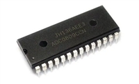
 ADC0809逐次逼近寄存器型模数转换器:资料手册参数分析

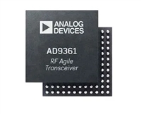
 AD9361捷变收发器:全面参数解析与关键特性概览

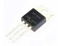
 IRF3205功率MOSFET:资料手册参数分析
