IDT29FCT2052AT/BT/CT
INDUSTRIALTEMPERATURERANGE
FASTCMOSOCTALREGISTEREDTRANSCEIVER
PINDESCRIPTION
Name
I/O
I/O
I/O
I
Description
EightbidirectionallinescarryingtheARegisterinputsorBRegisteroutputs
EightbidirectionallinescarryingtheBRegisterinputsorARegisteroutputs
A0-7
B0-7
CPA
CEA
Clock for the A Register. When CEA is LOW, data is entered into the A Register on the LOW-to-HIGH transition of the CPA signal.
I
ClockEnable forthe ARegister. WhenCEAis LOW, data is enteredintothe ARegisteronthe LOW-to-HIGHtransitionofthe CPAsignal. When
CEA is HIGH, the A Register holds its contents, regardless of CPA signal transitions.
OEB
I
OutputEnablefortheARegister. WhenOEBisLOW,theARegisteroutputsareenabledontotheB0-7 lines. WhenOEBisHIGH,theB0-7 outputs
areinthehigh-impedancestate.
CPB
I
I
Clock for the B Register. When CEB is LOW, data is entered into the B Register on the LOW-to-HIGH transition of the CPB signal.
CEB
ClockEnable forthe BRegister. WhenCEBis LOW, data is enteredintothe BRegisteronthe LOW-to-HIGHtransitionofthe CPBsignal. When
CEB is HIGH, the B Register holds its contents, regardless of CPB signal transitions.
OEA
I
OutputEnablefortheBRegister. WhenOEAisLOW,theBRegisteroutputsareenabledontotheA0-7 lines. WhenOEAisHIGH,theA0-7 outputs
areinthehigh-impedancestate.
DCELECTRICALCHARACTERISTICSOVEROPERATINGRANGE
FollowingConditionsApplyUnlessOtherwiseSpecified:
Industrial: TA = –40°C to +85°C, VCC = 5.0V ±5%
Symbol
VIH
VIL
Parameter
Input HIGH Level
Test Conditions(1)
Guaranteed Logic HIGH Level
Min.
2
Typ.(2)
—
Max.
—
Unit
V
Input LOW Level
Guaranteed Logic LOW Level
VCC = Max.
—
—
—
—
—
—
—
—
—
—
0.8
±1
±1
±1
±1
±1
–1.2
—
V
IIH
Input HIGH Current(4)
Input LOW Current(4)
High Impedance Output Current
VI = 2.7V
VI = 0.5V
VI = 2.7V
VI = 0.5V
—
µA
µA
µA
IIL
VCC = Max.
—
IOZH
IOZL
II
VCC = Max., VI = VCC (Max.)
—
(4)
(3-State Output pins)
—
Input HIGH Current(4)
Clamp Diode Voltage
Input Hysteresis
VCC = Max., VI = VCC (Max.)
VCC = Min., IIN = –18mA
—
µA
V
VIK
VH
–0.7
200
0.01
—
mV
µ A
ICC
Quiescent Power Supply Current
VCC = 3V
1
VIN = GND or VCC
OUTPUTDRIVECHARACTERISTICS
Symbol
Parameter
OutputLOWCurrent
Output HIGH Current
OutputHIGHVoltage
Test Conditions(1)
Min.
16
Typ.(2)
48
Max.
—
Unit
mA
mA
V
(3)
IODL
IODH
VOH
VCC = 5V, VIN = VIH or VIL, VOUT = 1.5V
(3)
VCC = 5V, VIN = VIH or VIL, VOUT = 1.5V
-16
2.4
-48
—
VCC = Min
IOH = –15mA
3.3
—
VIN = VIH or VIL
VCC = Min
VOL
Output LOWVoltage
IOL = 12mA
—
0.3
0.5
V
VIN = VIH or VIL
NOTES:
1. For conditions shown as Min. or Max., use appropriate value specified under Electrical Characteristics for the applicable device type.
2. Typical values are at VCC = 5.0V, +25°C ambient.
3. Not more than one output should be tested at one time. Duration of the test should not exceed one second.
4. The test limit for this parameter is ±5µA at TA = –55°C.
3


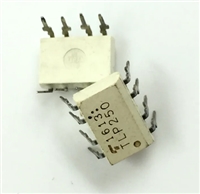
 TLP250光耦合器:资料手册参数分析

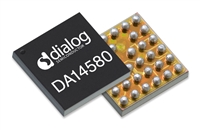
 DA14580 低功耗蓝牙系统级芯片(SoC):资料手册参数分析

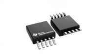
 INA226 高精度电流和功率监控器:资料手册参数分析

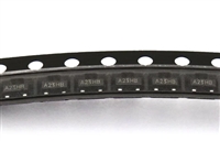
 SI2302 N沟道MOSFET:资料手册参数分析
