28F200BX-T/B, 28F002BX-T/B
1.0 PRODUCT FAMILY OVERVIEW
1.2 Main Features
Throughout this datasheet the 28F200BX refers to
both the 28F200BX-T and 28F200BX-B devices and
28F002BX refers to both the 28F002BX-T and
28F002BX-B devices. The 2-Mbit flash memory fam-
ily refers to both the 28F200BX and 28F002BX prod-
ucts. This datasheet comprises the specifications for
four separate products in the 2-Mbit flash memory
family. Section 1 provides an overview of the 2-Mbit
flash memory family including applications, pinouts
and pin descriptions. Sections 2 and 3 describe in
detail the specific memory organizations for the
28F200BX and 28F002BX products respectively.
Section 4 combines a description of the family’s
principles of operations. Finally Section 5 describes
the family’s operating specifications.
The 28F200BX/28F002BX boot block flash memory
family is a very high performance 2-Mbit (2,097,152
bit) memory family organized as either 128 KWords
(131,072 words) of 16 bits each or 256 Kbytes
(262,144 bytes) of 8 bits each.
Five Separately Erasable Blocks including a hard-
ware-lockable boot block (16,384 Bytes), two pa-
rameter blocks (8,192 Bytes each) and two main
blocks (1 block of 98,304 Bytes and 1 block of
131,072 Bytes) are included on the 2-Mbit family. An
erase operation erases one of the main blocks in
typically 2.4 seconds, and the boot or parameter
blocks in typically 1.0 second. Each block can be
independently erased and programmed 100,000
times.
PRODUCT FAMILY
The Boot Block is located at either the top
(28F200BX-T, 28F002BX-T) or the bottom
(28F200BX-B, 28F002BX-B) of the address map in
order to accommodate different microprocessor pro-
tocols for boot code location. The hardware locka-
ble boot block provides the most secure code stor-
age. The boot block is intended to store the kernel
code required for booting-up a system. When the
x8/x16 Products
28F200BX-T
x8-Only Products
28F002BX-T
28F200BX-B
28F002BX-B
1.1 Designing for Upgrade to
SmartVoltage Products
Ý
RP pin is between 11.4V and 12.6V the boot block
is unlocked and program and erase operations can
Today’s high volume boot block products are up-
gradable to Intel’s SmartVoltage boot block prod-
ucts that provide program and erase operation at 5V
Ý
be performed. When the RP pin is at or below 6.5V
the boot block is locked and program and erase op-
erations to the boot block are ignored.
or 12V V
and read operation at 3V or 5V V
.
PP
CC
Intel’s SmartVoltage boot block products provide the
following enhancements to the boot block products
described in this data sheet:
The 28F200BX products are available in the ROM/
EPROM compatible pinout and housed in the 44-
Lead PSOP (Plastic Small Outline) package and the
56-Lead TSOP (Thin Small Outline, 1.2mm thick)
Ý
1. DU pin is replaced by WP to provide a means
to lock and unlock the boot block with logic sig-
nals.
package as shown in Figures
3 and 4. The
28F002BX products are available in the 40-Lead
TSOP (1.2mm thick) package as shown in Figure 5.
2. 5V Program/Erase operation uses proven pro-
g
gram and erase techniques with 5V 10% ap-
plied to VPP.
The Command User Interface (CUI) serves as the
interface between the microprocessor or microcon-
troller and the internal operation of the 28F200BX
and 28F002BX flash memory products.
3. Enhanced circuits optimize performance at 3.3V
.
V
CC
Refer to the 2, 4 or 8 Mbit SmartVoltage Boot Block
Flash Memory Data Sheets for complete specifica-
tions.
Program and Erase Automation allows program
and erase operations to be executed using a two-
write command sequence to the CUI. The internal
Write State Machine (WSM) automatically executes
the algorithms and timings necessary for program
and erase operations, including verifications, there-
by unburdening the microprocessor or microcontrol-
ler. Writing of memory data is performed in word or
byte increments for the 28F200BX family and in byte
increments for the 28F002BX family typically within
9 ms which is a 100% improvement over current
flash memory products.
When you design with 12V V boot block products
PP
you should provide the capability in your board de-
sign to upgrade to SmartVoltage products.
Follow these guidelines to ensure compatibility:
Ý
1. Connect DU (WP on SmartVoltage products) to
a control signal or to V or GND.
CC
2. If adding a switch on V for write protection,
PP
switch to GND for complete write protection.
3. Allow for connecting 5V to V and disconnect
PP
12V from the V line, if desired.
PP
3


 SI2301 N沟道MOSFET:资料手册参数分析

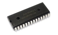
 ADC0809逐次逼近寄存器型模数转换器:资料手册参数分析

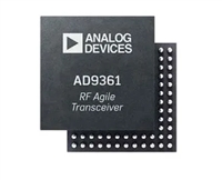
 AD9361捷变收发器:全面参数解析与关键特性概览

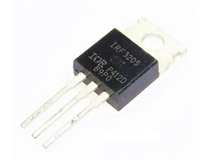
 IRF3205功率MOSFET:资料手册参数分析
