CCD area image sensor S7017 series
Electrical and optical characteristics (Ta=25 °C, unless otherwise noted)
ꢀ
Parameter
Symbol
Vsat
Remark
Min.
-
150
300
Typ.
Fw × Sv
300
Max.
Unit
V
Saturation output voltage
Full well
capacity
-
-
-
-
Vertical
Horizontal
4
-
*
Fw
Sv
ke
600
5
-
*
CCD conversion efficiency
1.8
2.2
-
µV/e
+25 °C
Dark current
0 °C
-
-
-
400
20
0.0015
3,000
150
0.01
6
-
*
DS
e /pixel/s
(MPP mode)
-70 °C
7
-
*
Readout noise
Nr
-
6
12
e rms
Line binning
Area scanning
Spectral response range
Photo response non-uniformity
Point defects
25,000
12,500
75,000
37,500
400 to 1,100
-
-
-
-
10
8
*
Dynamic range
DR
-
-
9
-
-
nm
%
λ
*
PRNU
10
*
-
-
-
-
-
-
0
0
0
11
*
Blemish
Cluster defects
Column defects
-
-
12
*
*4: Large horizontal full well for line binning operation.
*5: VOD=20 V , Load resistance=22 kΩ
*6: Dark current nearly doubles for every 5 to7 °C increase in temperature.
*7: -40 °C, operating frequency is 80 kHz.
*8: DR = Fw / Nr
*9: Measured at half of the full well capacity. PRNU (%) = noise / signal × 100, noise: fixed pattern noise (peak to peak)
*10: White spots > 3 % of full well at 0 °C after Ts=1 s, Black spots > 50 % reduction in response relative to adjacent
pixels
*11: continuous 2 to 9 point defects
*12: continuous >10 point defects
PIN connections
ꢀꢀ
Pin No.
1
Symbol
P-
Description
Remark
TE-cooler-
2
NC
3
SS
Substrate (GND)
4
NC
5
6
7
8
ISV
Test point (vertical input source)
Test point (vertical input gate-2)
Test point (vertical input gate-1)
Reset gate
Shorted to RD
Shorted to 0 V
Shorted to 0 V
IG2V
IG1V
RG
9
RD
Reset drain
10
11
12
13
14
15
16
17
18
19
20
21
22
23
24
25
26
27
28
OS
OD
OG
SG
Output transistor source
Output transistor drain
Output gate
Summing gate
TE-cooler+
Temperature sensor (hot side)
Temperature sensor (cool side)
Temperature sensor (cool side)
CCD horizontal register clock-2
CCD horizontal register clock-1
Test point (horizontal input gate-2)
Test point (horizontal input gate-1)
Test point (horizontal input source)
CCD vertical register clock-2
CCD vertical register clock-1
Transfer gate
Same timing as P2H
P+
TSH1
TSC1
TSC2
P2H
P1H
IG2H
IG1H
ISH
P2V
P1V
TG
NC
NC
Shorted to 0 V
Shorted to 0 V
Shorted to RD
Same timing as P2V *13
TSH2
Temperature sensor (hot side)
*13: TG is an isolation gate between vertical register and horizontal resister.
In standard operation, the same pulse of P2V should be applied to the TG.
3


 深入解析AD7606高性能多通道模数转换器:资料手册参数分析

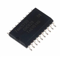
 74HC573三态非易失锁存器(Latch)资料手册参数分析

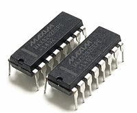
 MAX3232 RS-232电平转换器资料手册参数分析

 MAX485 RS-485/RS-422收发器资料手册参数分析
