LT3798
TA = 25°C, unless otherwise noted.
Efficiency vs Input Voltage
TYPICAL PERFORMANCE CHARACTERISTICS
Power Factor vs Input Voltage
100
1.00
PAGE 17 SCHEMAꢀIC:
UNIVERSAL
0.99
0.98
0.97
0.96
0.9±
0.94
0.93
0.92
90
80
70
PAGE 17 SCHEMAꢀIC:
UNIVERSAL
0.91
0.90
60
90 110 130 1±0 170 190 210 230 2±0 270
90
1±0 170 190 210 230 2±0 270
110 130
V
(VAC)
V
(VAC)
IN
IN
3798 G16
3798 G1±
PIN FUNCTIONS
CTRL1, CTRL2, CTRL3 (Pin 1, Pin 2, Pin 3): Current
Output Adjustment Pins. ꢀhese pins control the output
current. ꢀhe lowest value out of the three CꢀRL inputs is
compared to negative input of the operational amplifier.
FB (Pin 9): Voltage Loop Feedback Pin. FB is used to
regulate the output voltage by sampling the third wind-
ing. If the converter is used in current mode, the FB pin
will normally be at a voltage level lower than 1.2±V, and
will reach the steady state of 1.2±V if it detects an open
output condition.
V
(Pin 4): Voltage Reference Output Pin. ꢀypically 2V.
REF
ꢀhis pin drives a resistor divider for the CꢀRL pin, either
foranalogdimmingorfortemperaturelimit/compensation
of output load. Can supply up to 200μA.
DCM(Pin10):DiscontinuousConductionModeDetection
Pin. Connect a capacitor and resistor in series with this
pin to the third winding.
OVP (Pin 5): Overvoltage Protection. ꢀhis pin accepts a
DC voltage to compare to the sample and hold’s voltage
output information. When output voltage information is
above the OVP, the part divides the minimum switching
frequency by 8, around ±00Hz. ꢀhis protects devices con-
nected to the output. ꢀhis also allows the part to operate
with very little power consumption with no load to meet
energy star requirements.
V (Pin 11): Input Voltage. ꢀhis pin supplies current to
IN
the internal start-up circuitry and to the INꢀV LDO. ꢀhis
CC
pin must be locally bypassed with a capacitor. A 42V shunt
regulator is internally connected to this pin.
EN/UVLO(Pin12):Enable/UndervoltageLockout.Aresis-
tor divider connected to V is tied to this pin to program
IN
the minimum input voltage at which the Lꢀ3798 will turn
on. When below 1.2±V, the part will draw 60μA with most
of the internal circuitry disabled and a 10μA hysteresis
current will be pulled out of the EN/UVLO pin. When above
1.2±V, the part will be enabled and begin to switch and the
10μA hysteresis current is turned off.
VC (Pin 6): Compensation Pin for Internal Error Amplifier.
ConnectaseriesRCfromthispintogroundtocompensate
theswitchingregulator. A100pFcapacitorinparallelhelps
eliminate noise.
+
–
COMP , COMP (Pin 7, Pin 8): Compensation Pins for
InternalErrorAmplifier.Connectacapacitorbetweenthese
two pins to compensate the internal feedback loop.
INTV (Pin 13): Regulated Supply for Internal Loads
CC
and GAꢀE Driver. Supplied from V and regulates to 10V
IN
(typical). INꢀV must be bypassed with a 4.7μF capacitor
CC
placed close to the pin.
3798f
6


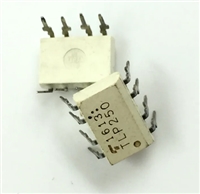
 TLP250光耦合器:资料手册参数分析

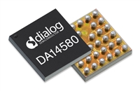
 DA14580 低功耗蓝牙系统级芯片(SoC):资料手册参数分析

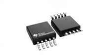
 INA226 高精度电流和功率监控器:资料手册参数分析

 SI2302 N沟道MOSFET:资料手册参数分析
