Data Sheet
June 1999
ORCA® Series 2
Field-Programmable Gate Arrays
■ Innovative, abundant, and hierarchical nibble-
oriented routing resources that allow automatic use of
internal gates for all device densities without sacrificing
performance
■ Upward bit stream compatible with the ORCA ATT2Cxx/
ATT2Txx series of devices
■ Pinout-compatible with new ORCA Series 3 FPGAs
■ TTL or CMOS input levels programmable per pin for the
OR2CxxA (5 V) devices
Features
■ High-performance, cost-effective, low-power
0.35 µm CMOS technology (OR2CxxA), 0.3 µm CMOS
technology (OR2TxxA), and 0.25 µm CMOS technology
(OR2TxxB), (four-input look-up table (LUT) delay less
than 1.0 ns with -8 speed grade)
■ High density (up to 43,200 usable, logic-only gates; or
99,400 gates including RAM)
■ Individually programmable drive capability:
12 mA sink/6 mA source or 6 mA sink/3 mA source
■ Built-in boundary scan (IEEE*1149.1 JTAG) and
3-state all I/O pins, (TS_ALL) testability functions
■ Multiple configuration options, including simple, low pin-
count serial ROMs, and peripheral or JTAG modes for in-
system programming (ISP)
■ Full PCI bus compliance for all devices
■ Supported by industry-standard CAE tools for design
entry, synthesis, and simulation with ORCA Foundry
Development System support (for back-end implementa-
tion)
■ Up to 480 user I/Os (OR2TxxA and OR2TxxB I/Os are
5 V tolerant to allow interconnection to both 3.3 V and
5 V devices, selectable on a per-pin basis)
■ Four 16-bit look-up tables and four latches/flip-flops per
PFU, nibble-oriented for implementing 4-, 8-, 16-, and/or
32-bit (or wider) bus structures
■ Eight 3-state buffers per PFU for on-chip bus structures
■ Fast, on-chip user SRAM has features to simplify RAM
design and increase RAM speed:
— Asynchronous single port: 64 bits/PFU
— Synchronous single port: 64 bits/PFU
— Synchronous dual port: 32 bits/PFU
■ New, added features (OR2TxxB) have:
— More I/O per package than the OR2TxxA family
— No dedicated 5 V supply (VDD5)
— Faster configuration speed (40 MHz)
— Pin selectable I/O clamping diodes provide 5V or 3.3V
PCI compliance and 5V tolerance
■ Improved ability to combine PFUs to create larger RAM
structures using write-port enable and 3-state buffers
■ Fast, dense multipliers can be created with the multiplier
mode (4 x 1 multiplier/PFU):
— 8 x 8 multiplier requires only 16 PFUs
— 30% increase in speed
— Full PCI bus compliance in both 5V and 3.3V PCI sys-
tems
■ Flip-flop/latch options to allow programmable priority of
synchronous set/reset vs. clock enable
■ Enhanced cascadable nibble-wide data path
capabilities for adders, subtractors, counters, multipliers,
and comparators including internal fast-carry operation
*
IEEE is a registered trademark of The Institute of Electrical and
Electronics Engineers, Inc.
Table 1. ORCA Series 2 FPGAs
Usable
Max User
RAM Bits
User
I/Os
Device
Gates*
# LUTs
Registers
Array Size
OR2C04A/OR2T04A
OR2C06A/OR2T06A
4,800—11,000
6,900—15,900
9,400—21,600
12,300—28,300
15,600—35,800
19,200—44,200
27,600—63,600
43,200—99,400
400
576
400
576
6,400
9,216
160
192
224
256
288
320
384
480
10 x 10
12 x 12
14 x 14
16 x 16
18 x 18
20 x 20
24 x 24
30 x 30
OR2C08A/OR2T08A
784
724
12,544
16,384
20,736
25,600
36,864
57,600
OR2C10A/OR2T10A
1024
1296
1600
2304
3600
1024
1296
1600
2304
3600
OR2C12A/OR2T12A
OR2C15A/OR2T15A/OR2T15B
OR2C26A/OR2T26A
OR2C40A/OR2T40A/OR2T40B
* The first number in the usable gates column assumes 48 gates per PFU (12 gates per four-input LUT/FF pair) for logic-only designs. The
second number assumes 30% of a design is RAM. PFUs used as RAM are counted at four gates per bit, with each PFU capable of
implementing a 16 x 4 RAM (or 256 gates) per PFU.


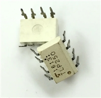
 TLP250光耦合器:资料手册参数分析

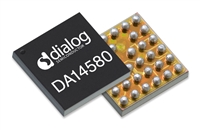
 DA14580 低功耗蓝牙系统级芯片(SoC):资料手册参数分析

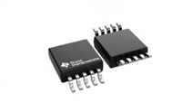
 INA226 高精度电流和功率监控器:资料手册参数分析

 SI2302 N沟道MOSFET:资料手册参数分析
