Propagation Delays
Figure 1 illustrates the calculations of a more useful propa-
Pin Descriptions
The following describes the function of all the MM82PC12
input/output pins. Some of these descriptions reference in-
ternal circuits.
gation delay. The figure uses a 5V supply with a tolerance of
a
g
tance of 100 pF. The AC Characteristics table depicts t
10%, ambient temperature of 25 C, and a load capaci-
§
,
PD
at 5V, 25 C, equalling 25 ns. Use the graph inFigure 1 to get
INPUT SIGNALS
§
Device Select (DS , DS : When DS is low and DS is high,
1
1
2
2
the degradation multiple for 150 pF. The number shown is
c
the device is selected. The output buffers are enabled and
the service request flip-flop is asynchronously reset
(cleared) when the device is selected.
1.09. The adjusted propagation delay is, therefore 25
1.09 or 27 ns.
Mode (MD): When MD is high (output mode), the output
buffers are enabled and the source of the data latch clock
input is the device selection logic (DS
DS ). When MD is
2
#
1
low (input mode), the state of the output buffers is deter-
mined by the device selection logic (DS DS ) and the
source of the data latch clock input is the strobe (STB) in-
put.
#
TL/C/5596–7
*Including jig and probe capacitance.
Output Test Circuit
1
2
for Propagation Delays
Strobe (STB): STB is used as the data latch clock input
when the mode (MD) input is low (input mode). STB is also
used to synchronously set the service request flip-flop,
which is negative edge triggered.
Data In (DI –DI ): Data In is the 8-bit data input to the data
8
1
latch, which consists of eight D-type flip-flops incorporating
a level sensitive clock. While the data latch clock input is
high, the Q output of each flip-flop follows the data input.
When the clock input returns low, the data latch stores the
data input. Clear (CLR) is only effective when the clock is
low (latch in the latched state).
TL/C/5596–8
Clear (CLR): When CLR is low, the data latch is reset
(cleared) if the clock is also low. The clock input high over-
rides the clear (CLR) input data latch reset. CLR being low
also resets the service request flip-flop. The service request
flip-flop is in the non-interrupting state when reset.
OUTPUT SIGNALS
Interrupt (INT): The interrupt pin goes low (interrupting
state) when either the service request flip-flop is synchro-
nously set by the strobe (STB) input or the device is select-
ed.
Data Out (DO –DO ): Data Out is the 8-bit data output of
8
1
data buffers, which are TRI-STATE, non-inverting stages.
These buffers have a common control line that either en-
ables the buffers to transmit the data from the data latch
outputs or disables the buffers by placing them in the high-
impedance state.
TL/C/5596–9
FIGURE 1. Normalized Typical Propagation Delay vs.
Load Capacitance
Reliability Information
Gate Count 108
Transistor Count 248
4


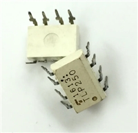
 TLP250光耦合器:资料手册参数分析

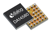
 DA14580 低功耗蓝牙系统级芯片(SoC):资料手册参数分析

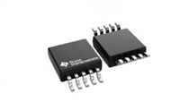
 INA226 高精度电流和功率监控器:资料手册参数分析

 SI2302 N沟道MOSFET:资料手册参数分析
