
 5秒后页面跳转

| 是否Rohs认证: | 符合 | 生命周期: | Obsolete |
| 零件包装代码: | SOIC | 包装说明: | SOP, SOP16,.3 |
| 针数: | 16 | Reach Compliance Code: | unknown |
| HTS代码: | 8542.39.00.01 | 风险等级: | 5.41 |
| 其他特性: | MIXED WITH 2-IN NOR & 2-IN NAND | 系列: | 4000/14000/40000 |
| JESD-30 代码: | R-PDSO-G16 | JESD-609代码: | e4 |
| 长度: | 10.2 mm | 负载电容(CL): | 50 pF |
| 逻辑集成电路类型: | INVERTER | 功能数量: | 6 |
| 输入次数: | 1 | 端子数量: | 16 |
| 最高工作温度: | 125 °C | 最低工作温度: | -55 °C |
| 封装主体材料: | PLASTIC/EPOXY | 封装代码: | SOP |
| 封装等效代码: | SOP16,.3 | 封装形状: | RECTANGULAR |
| 封装形式: | SMALL OUTLINE | 包装方法: | TAPE AND REEL |
| 峰值回流温度(摄氏度): | NOT SPECIFIED | 电源: | 5/15 V |
| Prop。Delay @ Nom-Sup: | 180 ns | 传播延迟(tpd): | 180 ns |
| 认证状态: | Not Qualified | 施密特触发器: | NO |
| 座面最大高度: | 2.05 mm | 子类别: | Gates |
| 最大供电电压 (Vsup): | 18 V | 最小供电电压 (Vsup): | 3 V |
| 标称供电电压 (Vsup): | 5 V | 表面贴装: | YES |
| 技术: | CMOS | 温度等级: | MILITARY |
| 端子面层: | Nickel/Palladium/Gold (Ni/Pd/Au) | 端子形式: | GULL WING |
| 端子节距: | 1.27 mm | 端子位置: | DUAL |
| 处于峰值回流温度下的最长时间: | NOT SPECIFIED | 宽度: | 5.275 mm |
| Base Number Matches: | 1 |
| 型号 | 品牌 | 获取价格 | 描述 | 数据表 |
| MC14572UBDG | ONSEMI |
获取价格 |
Hex Gate |

|
| MC14572UBDR2 | ONSEMI |
获取价格 |
Hex Gate |
|
| MC14572UBDR2 | MOTOROLA |
获取价格 |
Inverter, 4000/14000/40000 Series, 4-Func, 1-Input, CMOS, PDSO16, SOIC-16 |
|
| MC14572UBDR2G | ONSEMI |
获取价格 |
Hex Gate |
|
| MC14572UBF | ONSEMI |
获取价格 |
Hex Gate |
|
| MC14572UBFEL | ONSEMI |
获取价格 |
Hex Gate |
|
| MC14573 | MOTOROLA |
获取价格 |
CMOS MSI(PROGRAMMABLE DUAL OP AMP / DUAL COMPARATOR |
|
| MC14573D | MOTOROLA |
获取价格 |
CMOS MSI(PROGRAMMABLE DUAL OP AMP / DUAL COMPARATOR |
|
| MC14573P | MOTOROLA |
获取价格 |
CMOS MSI(PROGRAMMABLE DUAL OP AMP / DUAL COMPARATOR |
|
| MC145740 | MOTOROLA |
获取价格 |
Dual Tone Multiple Frequency Line Interface |
|
 STS5DNE30L资料手册解读:参数分析、特性与应用

 MDU1511资料手册解读:探索这款MOSFET的全面特性
 2SB1260资料手册解读:电气参数、产品特性
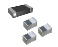 掌握电感选型:关键参数Q值全解析
工作时间:9:00-21:00
CEO邮箱:ceo@jiepei.com
投诉邮箱:tousu@jiepei.com


 浙公网安备 33010502006866号 浙ICP备10014259号-119
营业执照ICP证
浙公网安备 33010502006866号 浙ICP备10014259号-119
营业执照ICP证


