
 5秒后页面跳转

| 是否Rohs认证: | 符合 | 生命周期: | Transferred |
| 零件包装代码: | BGA | 包装说明: | BGA, |
| 针数: | 144 | Reach Compliance Code: | compliant |
| ECCN代码: | EAR99 | HTS代码: | 8542.39.00.01 |
| 风险等级: | 8.47 | 其他特性: | ALSO OPERATES IN ADJUSTABLE MODE FROM 0.6V TO 6V |
| 模拟集成电路 - 其他类型: | SWITCHING REGULATOR | 控制模式: | CURRENT-MODE |
| 控制技术: | PULSE FREQUENCY MODULATION | 最大输入电压: | 38 V |
| 最小输入电压: | 4.5 V | 标称输入电压: | 28 V |
| JESD-30 代码: | S-PBGA-B144 | 长度: | 15 mm |
| 功能数量: | 1 | 端子数量: | 144 |
| 最高工作温度: | 125 °C | 最低工作温度: | -55 °C |
| 标称输出电压: | 5.3 V | 封装主体材料: | PLASTIC/EPOXY |
| 封装代码: | BGA | 封装形状: | SQUARE |
| 封装形式: | GRID ARRAY | 峰值回流温度(摄氏度): | NOT SPECIFIED |
| 座面最大高度: | 5.21 mm | 表面贴装: | YES |
| 切换器配置: | PUSH-PULL | 温度等级: | MILITARY |
| 端子形式: | BALL | 端子节距: | 1.27 mm |
| 端子位置: | BOTTOM | 处于峰值回流温度下的最长时间: | NOT SPECIFIED |
| 宽度: | 15 mm | Base Number Matches: | 1 |
| 型号 | 品牌 | 获取价格 | 描述 | 数据表 |
| LTM4642 | Linear |
获取价格 |
Dual 10A or Single 20A μModule Regulator |

|
| LTM4642EY#PBF | Linear |
获取价格 |
LTM4642 - 20VIN, Dual 4A or Single 8A DC/DC µModule Regulator; Package: BGA; Pins |
|
| LTM4642IY#PBF | Linear |
获取价格 |
LTM4642 - 20VIN, Dual 4A or Single 8A DC/DC µModule Regulator; Package: BGA; Pins |
|
| LTM4643 | Linear |
获取价格 |
Ultrathin Quad μModule Regulator with Config |
|
| LTM4643 | ADI |
获取价格 |
20VIN, Dual 5A or Single 10A Step-Down DC/DC |
|
| LTM4643EV#PBF | Linear |
获取价格 |
LTM4643 - Ultrathin Quad µModule Regulator with Configurable 3A Output Array; Pac |
|
| LTM4643EY#PBF | Linear |
获取价格 |
LTM4643 - Ultrathin Quad µModule Regulator with Configurable 3A Output Array; Pac |
|
| LTM4643IV#PBF | Linear |
获取价格 |
LTM4643 - Ultrathin Quad µModule Regulator with Configurable 3A Output Array; Pac |
|
| LTM4643IY | Linear |
获取价格 |
LTM4643 - Ultrathin Quad µModule Regulator with Configurable 3A Output Array; Pac |
|
| LTM4643IY#PBF | Linear |
获取价格 |
LTM4643 - Ultrathin Quad µModule Regulator with Configurable 3A Output Array; Pac |
|
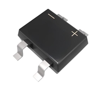 数据手册解读:MB10S引脚说明、电气参数

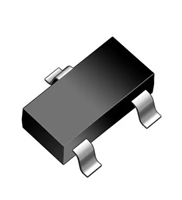 2N7002K资料解读:产品特性和型号推荐
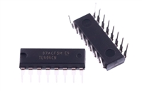 资料解读:TL494CN参数和引脚功能图说明
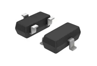 解读BAT54A数据手册:全面解析产品特性与应用
工作时间:9:00-21:00
CEO邮箱:ceo@jiepei.com
投诉邮箱:tousu@jiepei.com


 浙公网安备 33010502006866号 浙ICP备10014259号-119
营业执照ICP证
浙公网安备 33010502006866号 浙ICP备10014259号-119
营业执照ICP证


