
 5秒后页面跳转

| 型号 | 品牌 | 获取价格 | 描述 | 数据表 |
| LTC1481_1 | Linear |
获取价格 |
Ultralow Power RS485 Transceiver with Shutdown |

|
| LTC1481C | Linear |
获取价格 |
Ultra-Low Power RS485 Transceiver with Shutdown |
|
| LTC1481CN8 | Linear |
获取价格 |
Ultra-Low Power RS485 Transceiver with Shutdown |
|
| LTC1481CS8 | Linear |
获取价格 |
Ultra-Low Power RS485 Transceiver with Shutdown |
|
| LTC1481CS8#PBF | Linear |
获取价格 |
暂无描述 |
|
| LTC1481CS8#TR | Linear |
获取价格 |
暂无描述 |
|
| LTC1481I | Linear |
获取价格 |
Ultra-Low Power RS485 Transceiver with Shutdown |
|
| LTC1481IN8 | Linear |
获取价格 |
Ultra-Low Power RS485 Transceiver with Shutdown |
|
| LTC1481IS8 | Linear |
获取价格 |
Ultra-Low Power RS485 Transceiver with Shutdown |
|
| LTC1481IS8#PBF | Linear |
获取价格 |
暂无描述 |
|
 解读MMBT5401数据手册:电气参数及替换型号推荐

 深入解读BAV70数据手册:特性、应用、封装、电气参数及替换型号推荐
 74HC595D芯片引脚图及功能、参数介绍、替代型号推荐
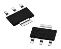 AMS1117-5.0数据手册:特性、引脚说明、参数与替代型号推荐
工作时间:9:00-21:00
CEO邮箱:ceo@jiepei.com
投诉邮箱:tousu@jiepei.com


 浙公网安备 33010502006866号 浙ICP备10014259号-119
营业执照ICP证
浙公网安备 33010502006866号 浙ICP备10014259号-119
营业执照ICP证


