LTC1069-6
U
U
U
PIN FUNCTIONS
only. Table 1 shows the clock’s low and high level thresh-
old value for a dual or single supply operation. A pulse
generator can be used as a clock source provided the high
level ON time is greater than 0.42µs (VS = ±5V). Sine
waves less than 100kHz are not recommended for clock
frequencies because, excessive slow clock rise or fall
times generate internal clock jitter. The maximum clock
rise or fall time is 1µs. The clock signal should be routed
from the right side of the IC package to avoid coupling into
any input or output analog signal path. A 1k resistor
between the clock source and the Clock Input (Pin 5) will
slow down the rise and fall times of the clock to further
reduce charge coupling (Figure 1).
1
8
7
AGND
V
V
OUT
OUT
2
+
–
–
+
V
V
V
V
0.1µF
0.1µF
LTC1069-6
3
4
6
5
NC
NC
V
V
IN
CLK
IN
ANALOG GROUND PLANE
STAR
DIGITAL
GROUND
1k
SYSTEM
GROUND
PLANE
CLOCK
SOURCE
1069-6 F03
Figure 3. Connections for Dual Supply Operation
Table 1. Clock Source High and Low Thresholds
NC (Pins 3, 6): No Connection. Pins 3 and 6 are not
connected to any internal circuitry; they should be tied to
ground.
POWER SUPPLY
HIGH LEVEL
1.5V
LOW LEVEL
0.5V
Dual Supply = ±5V
Single Supply = 10V
Single Supply = 5V
Single Supply = 3.3V
6.5V
5.5V
VIN (Pin4):FilterInputPin. TheFilterInputpinisinternally
connected to the inverting input of an op amp through a
50k resistor.
1.5V
0.5V
1.2V
0.5V
CLK (Pin 5): Clock Input Pin. Any TTL or CMOS clock
source with a square wave output and 50% duty cycle
(±10%) is an adequate clock source for the device. The
power supply for the clock source should not necessarily
be the filter’s power supply. The analog ground of the filter
shouldbeconnectedtotheclock’sgroundatasinglepoint
VOUT (Pin 8): Filter Output Pin. Pin 8 is the output of the
filter, and it can source 8mA or sink 1mA. The total
harmonic distortion of the filter will degrade when driving
coaxial cables or loads less than 20k without an output
buffer.
U
W U U
APPLICATIONS INFORMATION
2
Temperature Behavior
V
V
= SINGLE 3V
S
= 0.5V
IN
RMS
The power supply current of the LTC1069-6 has a positive
temperature coefficient. The GBW product of its internal
op amps is nearly constant and the speed of the device
doesnotdegradeathightemperatures. Figures4a, 4band
4c show the behavior of the passband of the device for
various supplies and temperatures. The filter has a pass-
band behavior which is temperature independent.
1
0
85°C
–40°C
f
f
= 500kHz
CLK
CUTOFF
–1
–2
= 10kHz
1
3
5
7
9
11 13 15 17 19 21
FREQUENCY (kHz)
1069-6 F04a
Figure 4a
6


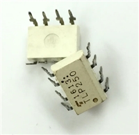
 TLP250光耦合器:资料手册参数分析

 DA14580 低功耗蓝牙系统级芯片(SoC):资料手册参数分析

 INA226 高精度电流和功率监控器:资料手册参数分析

 SI2302 N沟道MOSFET:资料手册参数分析
