LNK302/304-306
KEY FEATURES
TOPOLOGY
BASIC CIRCUIT SCHEMATIC
Low-Side
1. Output referenced to input
2. Positive output (VO) with respect to +VIN
3. Step up/down – VO > VIN or VO < VIN
4. Optocoupler feedback
Buck Boost –
Optocoupler
Feedback
+
LinkSwitch-TN
- Accuracy only limited by reference
choice
VIN
VO
- Low cost non-safety rated opto
- No pre-load required
5. Fail-safe – output is not subjected to input
voltage if the internal MOSFET fails
BP
FB
+
D
S
PI-3756-111903
Table 2 (cont). Common Circuit Configurations Using LinkSwitch-TN.
provides the lowest cost and highest efficiency converter. CCM
designs require a larger inductor and ultra-fast (trr ≤35 ns)
freewheeling diode in all cases. It is lower cost to use a larger
LinkSwitch-TNinMDCMthanasmallerLinkSwitch-TNinCCM
because of the additional external component costs of a CCM
design. However, ifthehighestoutputcurrentisrequired, CCM
should be employed following the guidelines below.
Feedback Diode D2
Diode D2 can be a low-cost slow diode such as the 1N400X
series, however it should be specified as a glass passivated type
to guarantee a specified reverse recovery time. To a first order,
the forward drops of D1 and D2 should match.
Inductor L1
Choose any standard off-the-shelf inductor that meets the
design requirements. A “drum” or “dog bone” “I” core
inductor is recommended with a single ferrite element due to
its low cost and very low audible noise properties. The typical
inductance value and RMS current rating can be obtained from
the LinkSwitch-TN design spreadsheet available within the
PI Expert design suite from Power Integrations. Choose L1
greater than or equal to the typical calculated inductance with
RMS current rating greater than or equal to calculated RMS
inductor current.
Topology Options
LinkSwitch-TN can be used in all common topologies, with or
withoutanoptocouplerandreferencetoimproveoutputvoltage
tolerance and regulation. Table 2 provide a summary of these
configurations. For more information see the Application
Note – LinkSwitch-TN Design Guide.
Component Selection
Referring to Figure 5, the following considerations may be
Capacitor C2
helpful in selecting components for a LinkSwitch-TN design.
The primary function of capacitor C2 is to smooth the inductor
current. The actual output ripple voltage is a function of this
capacitor’s ESR. To a first order, the ESR of this capacitor
shouldnotexceedtheratedripplevoltagedividedbythetypical
current limit of the chosen LinkSwitch-TN.
Freewheeling Diode D1
Diode D1 should be an ultra-fast type. For MDCM, reverse
recovery time trr ≤75 ns should be used at a temperature of
70°Corbelow. Slowerdiodesarenotacceptable,ascontinuous
mode operation will always occur during startup, causing high
leading edge current spikes, terminating the switching cycle
prematurely,andpreventingtheoutputfromreachingregulation.
If the ambient temperature is above 70 °C then a diode with
trr ≤35 ns should be used.
Feedback Resistors R1 and R3
The values of the resistors in the resistor divider formed by
R1 and R3 are selected to maintain 1.65 V at the FB pin. It is
recommended that R3 be chosen as a standard 1% resistor of
2kΩ. Thisensuresgoodnoiseimmunitybybiasingthefeedback
network with a current of approximately 0.8 mA.
For CCM an ultra-fast diode with reverse recovery time
trr ≤35 ns should be used. A slower diode may cause excessive
leading edge current spikes, terminating the switching cycle
prematurely and preventing full power delivery.
Feedback Capacitor C3
Capacitor C3 can be a low cost general purpose capacitor. It
provides a “sample and hold” function, charging to the output
voltage during the off time of LinkSwitch-TN. Its value should
be 10 μF to 22 μF; smaller values cause poorer regulation at
light load conditions.
Fast and slow diodes should never be used as the large reverse
recovery currents can cause excessive power dissipation in the
diode and/or exceed the maximum drain current specification
of LinkSwitch-TN.
27-7
Rev. I 11/08


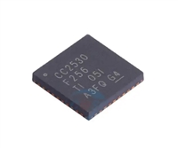
 CC2530无线微控制器:资料手册参数分析

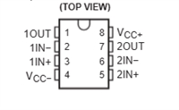
 NE5532双低噪声运算放大器:资料手册参数分析

 74LS138 3-to-8线解码器/多路复用器:资料手册参数分析

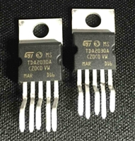
 TDA2030音频功率放大器:资料手册参数分析
