Input/Output Functional Descriptions
Symbol
Type
Function
CK0_t, CK0_c,
CK1_t, CK1_c
Clock: CK_t and CK_c are differential clock inputs. All address and control input signals
are sampled on the crossing of the positive edge of CK_t and negative edge of CK_c.
Input
Clock Enable: CKE HIGH activates and CKE LOW deactivates internal clock signals and
device input buffers and output drivers. Taking CKE LOW provides Precharge Power-
Down and Self-Refresh operation (all banks idle), or Active Power-Down (row Active in
any bank). CKE is aynchronous for Self-Refresh exit. After VREFCA and Internal DQ Vref
CKE0, CKE1
Input have become stable during the power on and initialization sequence, they must be
maintained during all operations (including Self-Refresh). CKE must be maintained high
throughout read and write accesses. Input buffers, excluding CK_t, CK_c, ODT and CKE,
are disabled during power-down. Input buffers, excluding CKE, are disabled during Self-
Refresh.
Chip Select: All commands are masked when CS_n is registered HIGH. CS_n provides for
Input external Rank selection on systems with multiple Ranks. CS_n is considered part of the
command code.
CS0_n, CS1_n,
CS2_n, CS3_n
Chip ID: Chip ID is only used for 3DS for 2,4,8 high stack via TSV to select each slice of
stacked component. Chip ID is considered part of the command code.
C0, C1
Input
On-Die Termination: ODT (registered HIGH) enables RTT_NOM termination resistance
internal to the DDR4 SDRAM. When enabled, ODT is only applied to each DQ, DQS_t,
DQS_c and DM_n/DBI_n/, signal. The ODT pin will be ignored if MR1 is programmed to
ODT0, ODT1
Input
disable RTT_NOM.
Activation Command Input: ACT_n defines the Activation command being entered along
Input with CS_n. The input into RAS_n/A16, CAS_n/A15 and WE_n/A14 will be considered as
Row Address A16, A15 and A14.
ACT_n
Command Inputs: RAS_n/A16, CAS_n/A15 and WE_n/A14 (along with CS_n) define the
command being entered. Those pins have multi function. For example, for activation
Input with ACT_n Low, these are Addresses like A16, A15, and A14. But for non-activation
command with ACT_n High, these are Command pins for Read, Write, and other
commands defined in command truth table.
RAS_n/A16,
CAS_n/A15,
WE_n/A14
Input Data Mask and Data Bus Inversion: DM_n is an input mask signal for write data.
Input data is masked when DM_n is sampled LOW coincident with that input data during
Input/ a Write access. DM_n is sampled on both edges of DQS. DM is muxed with DBI function.
Output DBI_n is an input/output identifing whether to store/output the true or inverted data. If
DBI_n is LOW. the data will be stored/output after inversion inside the DDR4 SDRAM and
not inverted if DBI_n is HIGH.
DM_n/DBI_n/
BG0, BG1
Bank Group Inputs: BG0 - BG1 define which bank group an Active, Read, Write, or
Precharge command is being applied. BG0 also determines which mode register is to be
accessed during a MRS cycle. x4/x8 SDRAM configurations have BG0 and BG1. x16
Input
based SDRAMs only have BG0.
Bank Address Inputs: BA0 - BA1 define to which bank an Active, Read, Write or
Input Precharge command is being applied. Bank address also determines which mode
register is to be accessed during a MRS cycle.
BA0, BA1
Rev. 1.1 / Aug.2019
6


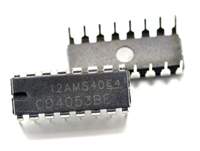
 CD4052资料手册参数详解、引脚配置说明

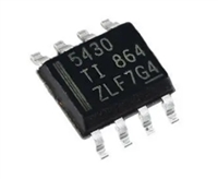
 一文带你了解TPS5430资料手册分析:参数介绍、引脚配置说明

 STM32F030C6芯片介绍:主要参数分析、引脚配置说明、功耗及封装

 PCF8591数据手册解读:参数、引脚说明
