HI-1565, HI-1566
PIN DESCRIPTIONS
PIN
(DIP/ESOIC)
SYMBOL
FUNCTION
DESCRIPTION
1
2
VDDA
BUSA
BUSA
RXENA
GNDA
VDDB
BUSB
BUSB
RXENB
GNDB
RXB
power supply
analog output
analog output
digital input
power supply
power supply
analog output
analog output
digital input
power supply
digital output
digital output
digital input
digital input
digital input
digital output
digital output
digital input
digital input
digital input
+5 volt power for channel A
MIL-STD-1533 bus driver A, positive signal
MIL-STD-1553 bus driver A, negative signal
Receiver A enable. If low, forces RXA and RXA low (HI-1565) or High (HI-1566)
Ground for channel A
3
4
5
6
+5 volt power for channel B
7
MIL-STD-1533 bus driver B, positive signal
MIL-STD-1553 bus driver B, negative signal
Receiver B enable. If low, forces RXB and RXB low (HI-1565) or High (HI-1566)
Ground for channel B
8
9
10
11
12
13
14
15
16
17
18
19
20
Receiver B output, inverted
RXB
Receiver B output, non-inverted
TXINHB
TXB
Transmit inhibit, channel B. If high BUSB, BUSB disabled
Transmitter B digital data input, non-inverted
Transmitter B digital data input, inverted
Receiver A output, inverted
TXB
RXA
RXA
Receiver A output, non-inverted
TXINHA
TXA
Transmit inhibit, channel A. If high BUSA, BUSA disabled
Transmitter A digital data input, non-inverted
Transmitter A digital data input, inverted
TXA
FUNCTIONAL DESCRIPTION
RECEIVER
The HI-1565 family of data bus transceivers contain differ-
ential voltage source drivers and differential receivers.
They are intended for applications using a MIL-STD-1553
A/B data bus. The device produces a trapezoidal output
waveform during transmission.
The receiver accepts bi-phase differential data from the
MIL-STD-1553 bus through the same direct or transformer
coupled interface as the transmitter. The receiver’s differ-
ential input stage drives a filter and threshold comparator
that produces CMOS/TTL data at the RXA/B and RXA/B
output pins.
TRANSMITTER
Data input to the device’s transmitter section is from the
complementary CMOS /TTL inputs TXA/B and TXA/B.
The transmitter accepts Manchester II bi-phase data and
converts it to differential voltages on BUSA/B and BUSA/B.
The transceiver outputs are either direct or transformer
coupled to the MIL-STD-1553 data bus. Both coupling
methods produce a nominal voltage on the bus of 7.5 volts
peak to peak.
Each set of receiver outputs can be independently forced
to a logic "0" (HI-1565) or logic “1” (HI-1566) by setting
RXENAor RXENB low.
MIL-STD-1553 BUS INTERFACE
A direct coupled interface (see Figure 2) uses a 1:2.5 ratio
isolation transformer and two 55 ohm isolation resistors
between the transformer and the bus.
The transmitter is automatically inhibited and placed in the
high impedance state when both TXA/B and TXA/B are ei-
ther at a logic “1” or logic “0” simultaneously. A logic “1” ap-
plied to the TXINHA/B input will force the transmitter to the
high impedance state, regardless of the state of TXA/B and
TXA/B.
In a transformer coupled interface (see Figure 3), the
transceiver is connected to a 1:1.79 isolation transformer
which in turn is connected to a 1:1.4 coupling transformer.
The transformer coupled method also requires two
coupling resistors equal to 75% of the bus characteristic
impedence (Zo) between the coupling transformer and the
bus.
HOLT INTEGRATED CIRCUITS
2


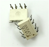
 TLP250光耦合器:资料手册参数分析

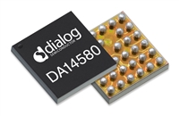
 DA14580 低功耗蓝牙系统级芯片(SoC):资料手册参数分析

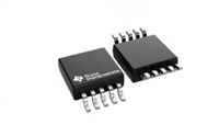
 INA226 高精度电流和功率监控器:资料手册参数分析

 SI2302 N沟道MOSFET:资料手册参数分析
