
 5秒后页面跳转

| 型号 | 品牌 | 描述 | 获取价格 | 数据表 |
| HD74LV1GWU04A | RENESAS | Dual Unbuffer Inverter |
获取价格 |

|
| HD74LV1GWU04ACME | RENESAS | Dual Unbuffer Inverter |
获取价格 |
|
| HD74LV20A | RENESAS | Dual 4-input Positive NAND Gates |
获取价格 |
|
| HD74LV20A | HITACHI | Dual 4-input Positive NAND Gates |
获取价格 |
|
| HD74LV20AFP | ETC | LOGIC GATE|DUAL 4-INPUT NAND|LV-CMOS|SOP|14PIN|PLASTIC |
获取价格 |
|
| HD74LV20AFPEL | RENESAS | Dual 4-input Positive NAND Gates |
获取价格 |
|
 CC2530无线微控制器:资料手册参数分析

 NE5532双低噪声运算放大器:资料手册参数分析
 74LS138 3-to-8线解码器/多路复用器:资料手册参数分析
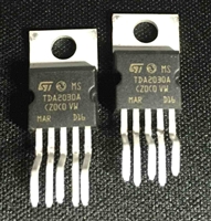 TDA2030音频功率放大器:资料手册参数分析
工作时间:9:00-21:00
CEO邮箱:ceo@jiepei.com
投诉邮箱:tousu@jiepei.com


 浙公网安备 33010502006866号 浙ICP备10014259号-119
营业执照ICP证
浙公网安备 33010502006866号 浙ICP备10014259号-119
营业执照ICP证


