Overload Protection
ISOLATION SPECIFICATIONS
Under normal operating conditions, the output
circuit of these products has no protection against
Item
Test conditions
Min
Typ
Typ
Max
Units
VDC
MΩ
Isolation voltage
Tested for 1 minute and 1 mA max
3000
1000
overload. The simplest method is to connect
a
Isolation resistance Test at 500VDC
self-recovery fuse in series at the input end or add a
circuit breaker to the circuit.
OUTPUT SPECIFICATIONS
Recommended circuit
Item
Test conditions
Min
0.2
Max
2
Units
W
If you want to further decrease the input/output
ripple, an “LC” filtering network may be connected to
the input and output ends of the DC/DC converter,
see (Figure 1).
Output power
(3.3V output)
(others output)
(3.3V output)
(5V output)
±1.5
±1.2
20
For Vin change
of ±1%
Line regulation
Load regulation
12
10
15
%
Dual Output
L
10% to 100% load
(9V output)
8.3
6.8
6.3
10
L
+Vo
Vin
(12V output)
(15V output)
10
Cout
0V
Cin
DC
DC
DC
DC
Cout
10
L
L
GND
-Vo
Output voltage accuracy
See tolerance envelope graph
Single Output
Vin
Temperature drift
Ripple& Noise*
100% full load
20MHz Bandwidth
0.03
%/°C
L
+Vo
0V
75
70
150 mVp-p
Cout
Cin
Switching frequency Full load, nominal input
*Test ripple and noise by “parallel cable” method. See detailed operation instructions at Testing of
KHz
GND
(Figure 1)
Power Converter section, application notes.
Note:
1. All specifications measured at TA=25°C, humidity<75%, nominal input voltage and rated output load
unless otherwise specified.
2. Dual output models unbalanced load: ±5%.
It should also be noted that the inductance and the
frequency of the “LC” filtering network should be
staggered with the DC/DC frequency to avoid mutual
interference. However, the capacitance of the output
filter capacitor must be proper. If the capacitance is
too big, a startup problem might arise. For every
channel of output, provided the safe and reliable
operation is ensured, the recommended capacitance
of its filter capacitor sees (Table 1).
TYPICAL CHARACTERISTICS
EXTERNAL CAPACITOR TABLE (TABLE 1)
Single
Vout
(VDC)
Dual
Vout
(VDC)
Cin
(uF)
Vin
(VDC)
Cout
(uF)
Cout
(uF)
Operating Temp.(oC)
5
12
24
-
4.7
2.2
1
3.3/5
9
10
4.7
2.2
1
±5
±9
4.7
2.2
1
OUTLINE DIMENSIONS & PIN CONNECTIONS
12
±12
±15
First Angle Projection
-
15
1
RECOMMENDED FOOTPRINT
Top view,grid:2.54*2.54mm(0.1*0.1inch)
diameter:1.00mm(0.039inch)
It’s not recommended to connect any external capacitor in
the application field with less than 0.5 watt output.
Dual Output
Side view
Output Voltage Regulation and Over-voltage
Protection Circuit
1
2
5
5
6
The simplest device for output voltage regulation,
over-voltage and over-current protection is a linear
voltage regulator with overheat protection that is
connected to the input or output end in series (Figure
Single Output
1
2
2).
0.90
(0.035)
Dual Output
Bottom view
+Vout
REG
Vin
REG
FOOTPRINT DETAILS
Single
0V
DC DC
GND
Dual
Pin
1
-Vout
REG
REG
Vin
Vin
GND
-Vo
Note:
Unit:mm(inch)
Pin section:0.50*0.30mm(0.020*0.012inch)
Pinsection tolerances: 0.10mm( 0.004inch)
General tolerances: 0.25mm ( 0.010inch)
Single Output
GND
2
5
+Vout
0V
0V
Vin
REG
No pin
+Vo
6
0V
DC DC
7
+Vo
GND
APPLICATION NOTE
(Figure 2)
No parallel connection or plug and play.
Requirement on output load
To ensure this module can operate efficiently and reliably, During operation, the
minimum output load is not less than 10% of the full load, and that this product should
never be operated under no load! If the actual output power is very small, please
connect a resistor with proper resistance at the output end in parallel to increase the load,
or use our company’s products with a lower rated output power (E_S-1W&F_S-1W).
MORNSUN reserves the copyright
Specifications subject to change without notice.
E_S-2W & F_S-2W
A/2-2008
Page 2 of 2


 MAX6675资料手册参数详解、引脚配置说明

 LM258引脚图及功能介绍、主要参数分析

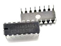
 CD4052资料手册参数详解、引脚配置说明

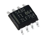
 一文带你了解TPS5430资料手册分析:参数介绍、引脚配置说明
