
 5秒后页面跳转

| 是否Rohs认证: | 符合 | 生命周期: | Obsolete |
| 包装说明: | BGA, | Reach Compliance Code: | compliant |
| 风险等级: | 5.76 | Is Samacsys: | N |
| JESD-30 代码: | S-PBGA-B956 | JESD-609代码: | e1 |
| 长度: | 40 mm | 可配置逻辑块数量: | 4697 |
| 端子数量: | 956 | 最高工作温度: | 85 °C |
| 最低工作温度: | 组织: | 4697 CLBS | |
| 封装主体材料: | PLASTIC/EPOXY | 封装代码: | BGA |
| 封装形状: | SQUARE | 封装形式: | GRID ARRAY |
| 峰值回流温度(摄氏度): | 245 | 可编程逻辑类型: | FIELD PROGRAMMABLE GATE ARRAY |
| 认证状态: | Not Qualified | 座面最大高度: | 3.5 mm |
| 最大供电电压: | 1.575 V | 最小供电电压: | 1.425 V |
| 标称供电电压: | 1.5 V | 表面贴装: | YES |
| 技术: | CMOS | 温度等级: | COMMERCIAL EXTENDED |
| 端子面层: | TIN SILVER COPPER | 端子形式: | BALL |
| 端子节距: | 1.27 mm | 端子位置: | BOTTOM |
| 处于峰值回流温度下的最长时间: | 40 | 宽度: | 40 mm |
| Base Number Matches: | 1 |
| 型号 | 品牌 | 获取价格 | 描述 | 数据表 |
| EP1S40B956I6 | INTEL |
获取价格 |
Field Programmable Gate Array, 41250-Cell, CMOS, PBGA956, 40 X 40 MM, 1.27 MM PITCH, BGA-9 |

|
| EP1S40B956I6 | ALTERA |
获取价格 |
Field Programmable Gate Array, 41250-Cell, CMOS, PBGA956, 40 X 40 MM, 1.27 MM PITCH, BGA-9 |
|
| EP1S40F1020C5 | ALTERA |
获取价格 |
Stratix Device Handbook, Volume 1 |
|
| EP1S40F1020C5ES | ALTERA |
获取价格 |
Field Programmable Gate Array, CMOS, PBGA1020, 33 X 33 MM, 1 MM PITCH, FBGA-1020 |
|
| EP1S40F1020C5N | ALTERA |
获取价格 |
Field Programmable Gate Array, 4697 CLBs, 41250-Cell, CMOS, PBGA1020, 33 X 33 MM, 1 MM PIT |
|
| EP1S40F1020C6 | ALTERA |
获取价格 |
Field Programmable Gate Array, 4697 CLBs, 41250-Cell, CMOS, PBGA1020, 33 X 33 MM, 1 MM PIT |
|
| EP1S40F1020C6N | ALTERA |
获取价格 |
Field Programmable Gate Array, 4697 CLBs, 41250-Cell, CMOS, PBGA1020, 33 X 33 MM, 1 MM PIT |
|
| EP1S40F1020C7 | ALTERA |
获取价格 |
Field Programmable Gate Array, 4697 CLBs, 41250-Cell, CMOS, PBGA1020, 33 X 33 MM, 1 MM PIT |
|
| EP1S40F1020I6N | INTEL |
获取价格 |
Field Programmable Gate Array, 4697 CLBs, 41250-Cell, CMOS, PBGA1020, 33 X 33 MM, 1 MM PIT |
|
| EP1S40F1020I6N | ALTERA |
获取价格 |
Field Programmable Gate Array, 4697 CLBs, 41250-Cell, CMOS, PBGA1020, 33 X 33 MM, 1 MM PIT |
|
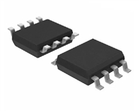 DS1135-8资料手册解读:深入探索高速硅定时电路的特性与应用

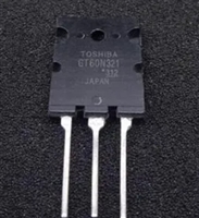 GT60N321资料手册解读:深入了解东芝第四代绝缘栅双极晶体管
 STS5DNE30L资料手册解读:参数分析、特性与应用
 MDU1511资料手册解读:探索这款MOSFET的全面特性
工作时间:9:00-21:00
CEO邮箱:ceo@jiepei.com
投诉邮箱:tousu@jiepei.com


 浙公网安备 33010502006866号 浙ICP备10014259号-119
营业执照ICP证
浙公网安备 33010502006866号 浙ICP备10014259号-119
营业执照ICP证


