DP83TC811R-Q1
www.ti.com.cn
ZHCSHX5A –NOVEMBER 2017–REVISED MARCH 2018
Pin Functions(1) (continued)
PIN
STATE(2)
DESCRIPTION
NAME
NO.
SERIAL MANAGEMENT INTERFACE
Management Data Clock: Synchronous clock to the MDIO serial management input and output
data. This clock may be asynchronous to the MAC transmit and receive clocks. The maximum clock
rate is 25 MHz. There is no minimum clock rate.
MDC
1
I
Management Data Input/Output: Bidirectional management data signal that may be sourced by the
management station or the PHY. This pin requires a pullup resistor.
MDIO
36
IO
Recommended to use a resistor between 2.2 kΩ and 9 kΩ.
CONTROL INTERFACE
Interrupt: Active-LOW output, which will be asserted LOW when an interrupt condition occurs. This
pin has a weak internal pullup. Register access is necessary to enable various interrupt triggers.
Once an interrupt event flag is set, register access is required to clear the interrupt event.
INT
2
PU, OD, O
Note: Power-on-RESET (POR) Done interrupt is enabled by default. POR Done interrupt can be
cleared by reading register INT_STAT3 Register 0x0018 – Interrupt Status Register #3.
This pin can be configured as an Active-HIGH output using register INT_TEST Register 0x0011 –
Interrupt Test Register.
Reset: Active-LOW input, which initializes or reinitializes the DP83TC811R-Q1. Asserting this pin
LOW for at least 1 μs will force a reset process to occur. All internal registers will reinitialize to their
default states as specified for each bit in the Register Maps section. All bootstrap pins are resampled
upon deassertion of reset.
RESET
EN
3
7
PU, I
PD, I
Enable: Active-HIGH input, which will disable the DP83TC811R-Q1 when pulled LOW and power
down all internal blocks. Disable state is equivalent to a power-down state.
This pin can be directly tied to VDDIO; enabling the device.
WAKE: Active-HIGH input, which wakes the PHY from SLEEP. Asserting this pin HIGH at power-up
will prevent the PHY from going to SLEEP.
WAKE
INH
8
PD, I
O
This pin can be directly tied to VDDIO to wake the device.
INH: Active-HIGH output, which will be asserted HIGH when the PHY is in SLEEP or DISABLED.
This pin is LOW for all other PHY states.
10
CLOCK INTERFACE
Reference Clock Input (MII and RGMII): Reference clock 25-MHz ±100 ppm-tolerance crystal or
oscillator input. The device supports either an external crystal resonator connected across pins XI
and XO, or an external CMOS-level oscillator connected to pin XI only and XO left floating.
Reference Clock Input (RMII): Reference clock 50-MHz ±100 ppm-tolerance CMOS-level oscillator
in RMII Slave mode. Reference clock 25-MHz ±100 ppm-tolerance crystal or oscillator in RMII Master
mode.
XI
5
4
I
This is a fail-safe pin. When the PHY is not powered, an external oscillator is allowed to be powered
and driving into this pin. Fail-safe prevents pin back-driving.
Reference Clock Output: XO pin is used for crystal only. This pin should be left floating when a
CMOS-level oscillator is connected to XI.
XO
O
LED/GPIO INTERFACE
LED_0 /
35
S, PD, IO
S, PD, IO
IO
LED_0: Link Status
GPIO_0
LED_1 /
6
LED_1: Link Status and BLINK for TX/RX Activity
Clock Output: 25-MHz reference clock
GPIO_1
CLKOUT /
16
GPIO_2
MEDIUM DEPENDENT INTERFACE
TRD_M
TRD_P
13
12
Differential Transmit and Receive: Bidirectional differential signaling configured for 100BASE-T1
operation, IEEE 802.3bw compliant.
IO
JTAG (IEEE 1149.1)
Test Clock: Primary clock source for all test logic input and output. This pin is controlled by the
testing entity.
TCK
17
PU, I
This pin can be left unconnected if not used.
Copyright © 2017–2018, Texas Instruments Incorporated
5


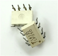
 TLP250光耦合器:资料手册参数分析

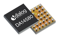
 DA14580 低功耗蓝牙系统级芯片(SoC):资料手册参数分析

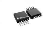
 INA226 高精度电流和功率监控器:资料手册参数分析

 SI2302 N沟道MOSFET:资料手册参数分析
