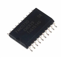
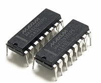
+/+…when timing is critical
C9809B
Low EMI Clock Generator for Intel 133MHz/3DIMM Chipset Systems
Preliminary
Pin Description
PIN No.
Pin Name
I/O TYPE
O
I/O PD
Description
1
4
2.5V IOAPIC clock outputs. See fig.3 p.4 for timing relationship.
This is a bi-directional pin (see app. note, p.6). At power up, it is an input pin
Sel1 for selecting the CPU/SDRAM frequencies (see table 1 p.1). When the
power reaches the rail, the state of Sel1 is latched, and this pin becomes REF,
a buffer output of the signal applied at Xin, typically 14.318MHz.
On-chip reference oscillator input pin. Requires either an external parallel
resonant crystal (nominally 14.318 MHz) or externally generated reference
signal
IOAPIC
SEL1/REF
6
I
OSC1
XIN
7
O
On-chip reference oscillator pin. Drives an external parallel resonant crystal.
When an externally generated reference signal is used at Xin, this pin remains
unconnected.
XOUT
14
VD
D
PD
PD
This is a bi-directional pin (see app. note, p.6). At power up, it is an input pin
Sel3 for frequency selection (see table 1 p.1). When the power reaches the
rail, the state of Sel3 is latched, and this pin becomes PCI0 clock output.
PCI clock outputs. They are Synchronous to CPU clocks. See fig.3, p.4
3.3V Fixed 66.6 MHz clock outputs. See fig.3 page 4.
This is a bi-directional pin (see app. note, p.6). At power up, it is an input pin
Sel2 for frequency selection (see table 1 p.1). When the power reaches the
rail, the state of Sel2 is latched, and this pin becomes a fixed 48MHz clock
output for USB.
SEL3 / PCI0
15, 16, 19, 20
10, 11, 12
28
O
O
O
PCI(1..4)
3V66(0:2)
SEL2 / USB
29
21
O
I
3.3V Fixed 48 MHz clock outputs
DOT
SEL0
PU1
3.3V LVTTL inputs for frequency selection, see table 1 page 1. SEL0 also
controls TS# functionality if TS# is 0 at power up (see pg. 7).
Serial data input pin. Conforms to the Philips I2C specification of a Slave
Receive/Transmit device. This pin is an input when receiving data. It is an
open drain output when acknowledging or transmitting data. See I2C function
description, pp.8, 9, 10.
25
I
SDATA
24
30
I
I
Serial clock input pin. Conforms to the Philips I2C specification.
This is a dual function pin. During power up, if TS# is low, it serves as a
Tristate control (TS#). Once high, this pin becomes a Power Down control
(PD#). See page 7 for detailed description.
SCLK
TS# / PD#
PU2
31,34,35,38,
39,40,41,44,
45,46,47,50,
51
53, 54
5,9,17,27
23
O
O
3.3V SDRAM DIMM clocks. See table1, p.1 for frequency selection. See fig.3,
SDRAM
(0:12)
page 4 for timing relationship and I2C Byte3, Bit0.
2.5V Host clock outputs. See table 1 p. 1 for frequency selection.
3.3V Common Power Supply
Analog circuitry 3.3V Power Supply
CPU(0:1)
VDD
VDDA
22
55, 2
3,8,13,18,26,3
2,36,42,48,
52,56
Analog circuitry power supply Ground pins.
2.5V Power Supply for CPU(0:1) and IOAPIC clock respectively.
Common Ground pins.
VSSA
VDDC,VDDI
VSS
-
-
33,37,43,49
3.3V power support for SDRAM clock output drivers.
VDDS
A bypass capacitor (0.1µF) should be placed as close as possible to each positive power pin. If these bypass capacitors are not close to
the pins their high frequency filtering characteristic will be cancelled by the lead inductance of the traces.
PU1 = Internal Pull-Up. Typical 250KΩ (range 200KΩ to 500KΩ), PU2 = Internal Pull-up. Typical 50KΩ (range 25KΩ to 75KΩ)
PD = Internal Pull-Down. Typical 50KΩ (range 25KΩ to 75KΩ)
INTERNATIONAL MICROCIRCUITS, INC. 525 LOS COCHES ST.,
MILPITAS, CA 95035, USA. TEL: 408-263-6300, FAX 408-263-6571
http://www.imicorp.com
Rev 1.2
3/8/2000
Page 2 of 20


 深入解析AD7606高性能多通道模数转换器:资料手册参数分析

 74HC573三态非易失锁存器(Latch)资料手册参数分析

 MAX3232 RS-232电平转换器资料手册参数分析

 MAX485 RS-485/RS-422收发器资料手册参数分析
