CERAMIC CHIP CAPACITORS
Packaging Information
Punched Carrier (Paper Tape) Configuration (Ceramic Chips Only):
10 pitches cumulative
P0
tolerance on tape
± 0.2 (± 0.008)
T
D0
P2
E
Top
Tape
Cover
A0
Bottom
Tape
Cover
F
W
B0
G2
T1
P1
Center lines
of cavity
Max. Cavity Size
See Note 1
Table 1
User Direction of Feed
Table 1: 8 & 12mm PunchedTape
(Metric Dimensions Will Govern)
Constant Dimensions - Millimeters (Inches)
Tape
Size
D
P
P
T
G
G
2
E
R Min.
0
0
2
1
1
8mm
and
12mm
1.5
1.75 ± 0.10
4.0 ± 0.10
2.0 ± 0.05
0.10 0.75 0.75 25 (.984)
(.004) (.030) (.030) See Note 2
+0.10, -0.0
(.059
(.069 ± 0.004) (.157 ± 0.004) (.079 ± 0.002) Max. Min. Min.
Table 1
+0.004, -0.0)
Table 1: 8 & 12mm PunchedTape
(Metric Dimensions Will Govern)
Variable Dimensions - Millimeters (Inches)
Tape
Size
P
W
A B
0 0
T
F
1
8mm
1/2
2.0 ± 0.10
1.1mm (.043)
Max. for Paper
Base Tape and
1.6mm (.063)
Max. for Non-
Paper Base
(.079 ± .004)
3.5 ± 0.05
8.0 ± ±0.3
See Note 1
Table 1
Pitch See Require-
ments
(.138 ± .002)
(.315 ± ±0.012)
Section 3.3 (d)
8mm
4.0 ± 0.10
(0.157 ± .004)
Compositions.
See Note 3.
12mm
12mm
4.0 ± 0.10
5.5 ± 0.05
12.0 ± 0.3
(0.157 ± .004)
8.0 ± 0.10
(.217 ± .002)
(.472 ± .012)
Double (0.315 ± .004)
Pitch
Note:
1. A , B and T determined by the maximum dimensions to the ends of the terminals extending from the
0
0
body and/or the body dimensions of the component. The clearance between the ends of the terminals or
body of the component to the sides and depth of the cavity (A , B and T) must be within 0.05mm (.002)
0
0
minimum and 0.50mm (.020) maximum. The clearance allowed must also prevent rotation of the component
within the cavity of not more than 20 degrees (see sketches A and B).
2. Tape with components shall pass around radius "R" without damage.
3. KEMET nominal thicknesses are: 0402 = 0.6mm and all others 0.95mm minimum.
Sketch C:
Component Rotation - Top View
Maximum
Sketch B:
R
(Min.)
Max. Component
Rotation - Front
component rotation.
Sketch A:
Bending Radius
See Note 2
Table 1
20°
Cross Sectional View
Typical
component
center line
20°
96
©KEMET Electronics Corporation, P.O. Box 5928, Greenville, S.C. 29606, (864) 963-6300


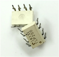
 TLP250光耦合器:资料手册参数分析

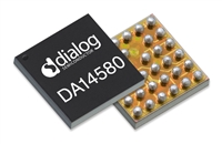
 DA14580 低功耗蓝牙系统级芯片(SoC):资料手册参数分析

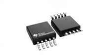
 INA226 高精度电流和功率监控器:资料手册参数分析

 SI2302 N沟道MOSFET:资料手册参数分析
