Ceramic
BFCN-2555+
Bandpass Filter
50Ω
2500 to 2610 MHz
Maximum Ratings
Features
• Good VSWR, 1.6:1 typ @ passband
• Small size
Operating Temperature
Storage Temperature
RF Power Input*
-55oC to 100oC
-55oC to 100oC
1.5W at 25oC
CASE STYLE: FV1206-1
• Temperature stable
• LTCC construction
* Passband rating, derate linearly to 0.25W at 100oC ambient.
+RoHS Compliant
Permanent damage may occur if any of these limits are exceeded.
Applications
The +Suffix identifies RoHS Compliance. See our web site
for RoHS Compliance methodologies and qualifications
• Harmonic rejection
• Transmitters / receivers
Pin Connections
RF IN
1
3
Bandpass Filter Electrical Specifications1,2 (TAMB= 25 C)
O
RF OUT
GROUND
2,4,5,6
CENTER
FREQ.
(MHz)
PASSBAND
(MHz)
(Loss < 7dB)
STOPBANDS (MHz)
VSWR (:1)
Outline Drawing
Loss > 20dB
Loss 30dB Typ
F5 F6
2000 3250 - 5500
Passband
Typ. Max.
1.6 2.8
Stopband
Typ.
Fc
F1 - F2
F3
F4
2555
2500 - 2610
1970
3200
20
1. Measured on Mini-Circuits Characterization Test Board TB-285.
2. This filter is not intended for use as a DC Blocking circuit element. In Application where DC voltage is present at either input
or output ports, blocking capacitors are required at the corresponding RF port.
Typical Frequency Response
Functional Schematic
RF IN
RF OUT
30
PCB Land Pattern
20
7
F5 F3 F1
F2 F4 F6
FREQUENCY (MHz)
Typical Performance Data at 25oC
Frequency
(MHz)
Insertion Loss
(dB)
VSWR
(:1)
Suggested Layout,
±
Tolerance to be within .002
50
200
500
1000
1970
2000
2200
81.46
82.15
62.32
52.18
37.86
36.18
20.62
289.53
124.09
75.53
56.04
23.49
21.73
9.58
inch
Outline Dimensions (
)
F
.011
0.28
mm
A
B
.063
C
.035
D
.024
E
.126
.022
0.56
3.20
1.60
0.89
0.61
G
.039
0.99
H
.024
J
.042
K
.123
wt.
grams
2300
2350
2500
2555
2610
2850
10.23
6.16
3.78
3.73
3.87
7.85
3.53
1.78
1.28
1.35
1.60
1.33
0.61
1.07
3.12
.020
Demo Board MCL P/N: TB-285
Suggested PCB Layout (PL-158)
6X ø.015 PTH
FOR GROUND
2920
3000
3200
3250
3700
4500
5500
14.80
24.74
39.85
40.88
44.06
39.38
29.82
3.09
6.51
.012
14.50
15.67
23.49
28.03
27.59
PACKAGE
OUTLINE
.010 TYP
.073
.012
PIN 1
BFCN-2555+
BFCN-2555+
INSERTION LOSS
VSWR
100
80
60
40
20
0
1000
100
10
1.6
1.5
1.4
1.3
1.2
4.0
3.9
3.8
.055
.044 ± .002
TRACE WIDTH, 2 PL.
(SEE NOTE BELOW)
3.7
.034
.010 TYP
.017
2500 2528 2555 2583 2610
2500 2528 2555 2583 2610
NOTES:
1. TRACE WIDTH IS SHOWN FOR ROGERS RO4350B WITH DIELECTRIC
THICKNESS .020” ± .0015”. COPPER: 1/2 OZ. EACH SIDE.
FOR OTHER MATERIALS TRACE WIDTH MAY NEED TO BE MODIFIED.
2. BOTTOM SIDE OF THE PCB IS CONTINUOUS GROUND PLANE.
DENOTES PCB COPPER LAYOUT WITH SMOBC
(SOLDER MASK OVER BARE COPPER)
1
0
1000
2000
3000
4000
5000
6000
0
1000
2000
3000
4000
5000
6000
DENOTES COPPER LAND PATTERN FREE OF SOLDER MASK
FREQUENCY (MHz)
FREQUENCY (MHz)
Notes
A. Performance and quality attributes and conditions not expressly stated in this specification document are intended to be excluded and do not form a part of this specification document.
B. Electrical specifications and performance data contained in this specification document are based on Mini-Circuit’s applicable established test performance criteria and measurement instructions.
C. The parts covered by this specification document are subject to Mini-Circuits standard limited warranty and terms and conditions (collectively, “Standard Terms”); Purchasers of this part are entitled
to the rights and benefits contained therein. For a full statement of the Standard Terms and the exclusive rights and remedies thereunder, please visit Mini-Circuits’ website at www.minicircuits.com/MCLStore/terms.jsp
REV. C
M151121
EDR-8495F1
BFCN-2555+
RAV
161102
Page 1 of 1
®
Mini-Circuits
www.minicircuits.com P.O. Box 350166, Brooklyn, NY 11235-0003 (718) 934-4500 sales@minicircuits.com

 5秒后页面跳转


 NE5532双低噪声运算放大器:资料手册参数分析

 74LS138 3-to-8线解码器/多路复用器:资料手册参数分析
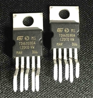 TDA2030音频功率放大器:资料手册参数分析
 74HC595移位寄存器芯片:参数深入解析与应用实践指南


 浙公网安备 33010502006866号 浙ICP备10014259号-119
营业执照ICP证
浙公网安备 33010502006866号 浙ICP备10014259号-119
营业执照ICP证


