
 5秒后页面跳转

| 是否Rohs认证: | 符合 | 生命周期: | Active |
| 包装说明: | 5 X 5 MM, 0.65 MM PITCH, MO-220, QFN-24 | Reach Compliance Code: | compliant |
| ECCN代码: | EAR99 | HTS代码: | 8542.39.00.01 |
| 风险等级: | 5.25 | JESD-30 代码: | S-XQCC-N24 |
| 长度: | 5 mm | 功能数量: | 1 |
| 端子数量: | 24 | 最高工作温度: | 85 °C |
| 最低工作温度: | -40 °C | 封装主体材料: | UNSPECIFIED |
| 封装代码: | HVQCCN | 封装等效代码: | LCC24,.19SQ,25 |
| 封装形状: | SQUARE | 封装形式: | CHIP CARRIER, HEAT SINK/SLUG, VERY THIN PROFILE |
| 电源: | 2.5/3.3 V | 认证状态: | Not Qualified |
| 筛选级别: | AEC-Q100 | 座面最大高度: | 1 mm |
| 子类别: | Other Telecom ICs | 最大压摆率: | 0.0141 mA |
| 标称供电电压: | 3 V | 表面贴装: | YES |
| 电信集成电路类型: | TELECOM CIRCUIT | 温度等级: | INDUSTRIAL |
| 端子形式: | NO LEAD | 端子节距: | 0.65 mm |
| 端子位置: | QUAD | 宽度: | 5 mm |
| Base Number Matches: | 1 |
| 型号 | 品牌 | 获取价格 | 描述 | 数据表 |
| ATA5773-PXQW | ATMEL |
获取价格 |
Microcontroller with UHF ASK/FSK Transmitter |

|
| ATA5774 | ATMEL |
获取价格 |
Microcontroller with UHF ASK/FSK Transmitter |
|
| ATA5774C | MICROCHIP |
获取价格 |
A highly flexible programmable ASK/FSK transmitter that combines an high-performance low p |
|
| ATA5774C-PXQW | MICROCHIP |
获取价格 |
Telecom Circuit, 1-Func |
|
| ATA5774-PXQW | ATMEL |
获取价格 |
Microcontroller with UHF ASK/FSK Transmitter |
|
| ATA5780N-PNQW | ATMEL |
获取价格 |
Telecom Circuit, 1-Func, PQCC32, |
|
| ATA5780N-WNQW | ATMEL |
获取价格 |
Telecom Circuit, 1-Func, 5 X 5 MM, 0.50 MM PITCH, LEAD FREE, VQFN-32 |
|
| ATA5780N-WNQW | MICROCHIP |
获取价格 |
Telecom Circuit, 1-Func |
|
| ATA5780-PNQW | ATMEL |
获取价格 |
Telecom Circuit, 1-Func, 5 X 5 MM, 0.50 MM PITCH, LEAD FREE, VQFN-32 |
|
| ATA5781 | ATMEL |
获取价格 |
AVR microcontroller core with 1Kbyte SRAM and 24Kbyte RF library in firmware (ROM) |
|
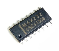 解读MAX232数据手册:全面剖析与应用推荐

 ATMEGA128数据手册解读:电气参数、引脚图
 温度传感器的常见故障及处理方法
 如何用万用表的欧姆档来辨别二极管的阴阳极
工作时间:9:00-21:00
CEO邮箱:ceo@jiepei.com
投诉邮箱:tousu@jiepei.com


 浙公网安备 33010502006866号 浙ICP备10014259号-119
营业执照ICP证
浙公网安备 33010502006866号 浙ICP备10014259号-119
营业执照ICP证


