AS1330
Datasheet ꢀ Pin Assignments
4 Pin Assignments
Figure 2. Pin Assignments (Top View)
8 VIN
SENSE
FB
1
2
3
7 VOUT
6 SW
AS1330
EN
5 GND
POK 4
9
Pin Descriptions
Table 1. Pin Descriptions
Pin Number
Pin Name
Description
Sense Input. Represents the input for the PowerꢀOK behavior. This input can be used to supervise
the input or the output voltage via a resistor divider. If connected to GND the POK output is related to
VOUT.
1
SENSE
Feedback Pin. Feedback input to the gm error amplifier. Connect a resistor divider tap to this pin. The
output voltage can be adjusted from 1.8 to 3.3V by: VOUT = 0.8V[1 + (R1/R2)]
If the fixed output voltage version is used, connect this pin to VOUT.
Active-High Enable Input. A logic LOW reduces the supply current to < 1ꢁA.
Connect to pin VIN for normal operation.
2
3
FB
EN
Power-OK Output. ActiveꢀHigh, openꢀdrain output indicates an outꢀofꢀregulation condition. Connect
a 100kΩ pullꢀup resistor to pin OUT for logic levels. Leave this pin unconnected if the PowerꢀOK
feature is not used.
4
POK
Low Level: VOUT is out of Regulation
High Level: VOUT is within Regulation
Signal and Power Ground. Provide a short, direct PCB path between this pin and the negative side
of the output capacitor(s).
5
6
GND
SW
Switch Pin. Connect an inductor between this pin and VIN. Keep the PCB trace lengths as short and
wide as is practical to reduce EMI and voltage overshoot. If the inductor current falls to zero, or pin
EN is low, an internal 100Ω antiꢀringing switch is connected from this pin to VIN to minimize EMI.
Note: An optional Schottky diode can be connected between this pin and VOUT.
Output Voltage. Bias is derived from VOUT when VOUT exceeds VIN. PCB trace length from VOUT
to the output filter capacitor(s) should be as short and wide as is practical.
Input Voltage. The AS1330 gets its startꢀup bias from VIN unless VOUT exceeds VIN, in which case
the bias is derived from VOUT. Thus, once started, operation is completely independent from VIN.
Operation is only limited by the output power level and the internal series resistance of the supply.
Exposed Pad. The exposed pad must be connected to GND. Ensure a good connection to the PCB
to achieve optimal thermal performance.
7
8
VOUT
VIN
9
www.austriamicrosystems.com/DCꢀDC_StepꢀUp/AS1330
Revision 1.06
2 ꢀ 17


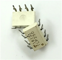
 TLP250光耦合器:资料手册参数分析

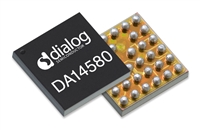
 DA14580 低功耗蓝牙系统级芯片(SoC):资料手册参数分析

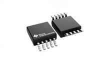
 INA226 高精度电流和功率监控器:资料手册参数分析

 SI2302 N沟道MOSFET:资料手册参数分析
