Data Sheet
ADuM3224/ADuM4224
SPECIFICATIONS
ELECTRICAL CHARACTERISTICS—5 V OPERATION
All voltages are relative to their respective ground. 4.5 V ≤ VDD1 ≤ 5.5 V, 4.5 V ≤ VDDA ≤ 18 V, 4.5 V ≤ VDDB ≤ 1 8 V, unless stated otherwise.
All minimum/maximum specifications apply over TJ = −40°C to +125°C. All typical specifications are at TJ = 25°C, VDD1 = 5 V, V DDA
DDB = 12 V. Switching specifications are tested with CMOS signal levels.
=
V
Table 1.
Parameter
Symbol
Min
Typ
Max
Unit
Test Conditions/Comments
DC SPECIFICATIONS
Input Supply Current, Quiescent
Output Supply Current, Per Channel, Quiescent
Supply Current at 1 MHz
VDD1 Supply Current
IDDI(Q)
1.4
2.3
2.4
3.2
mA
mA
IDDO(Q)
IDD1(Q)
1.6
5.6
2.5
8.0
mA
mA
µA
V
Up to 1 MHz, no load
Up to 1 MHz, no load
0 V ≤ VIA, VIB ≤ VDD1
VDDA/VDDB Supply Current
Input Currents
IDDA(Q)/IDDB(Q)
IIA, IIB
−1
+0.01 +1
Logic High Input Threshold
Logic Low Input Threshold
Logic High Output Voltages
VIH
0.7 × VDD1
VIL
0.3 × VDD1
0.15
V
VOAH, VOBH
VDDA
V
/
VDDA
DDB − 0.1 VDDB
/
V
IOx = −20 mA, VIx = VIxH
IOx = +20 mA, VIx = VIxL
Logic Low Output Voltages
Undervoltage Lockout, VDDA/VDDB Supply
A Grade
VOAL, VOBL
0.0
V
Positive Going Threshold
Negative Going Threshold
Hysteresis
VDDAUV+, VDDBUV+
VDDAUV−, VDDBUV−
VDDAUVH, VDDBUVH
4.1
4.4
V
V
V
3.2
5.7
8.9
3.6
0.5
B Grade
Positive Going Threshold
Negative Going Threshold
Hysteresis
VDDAUV+, VDDBUV+
VDDAUV−, VDDBUV−
VDDAUVH, VDDBUVH
6.9
6.2
0.7
7.4
V
V
V
C Grade
Positive Going Threshold
Negative Going Threshold
Hysteresis
VDDAUV+, VDDBUV+
VDDAUV−, VDDBUV−
VDDAUVH, VDDBUVH
IOA(SC), IOB(SC)
ROA, ROB
10.5
9.6
0.9
4.0
1.1
0.6
11.1
V
V
V
Output Short-Circuit Pulsed Current1
Output Pulsed Source Resistance
Output Pulsed Sink Resistance
SWITCHING SPECIFICATIONS
Pulse Width2
Maximum Data Rate3
Propagation Delay4
2.0
0.3
0.3
A
Ω
Ω
VDDA/VDDB = 12 V
VDDA/VDDB = 12 V
VDDA/VDDB = 12 V
3.0
3.0
ROA, ROB
PW
50
1
ns
CL = 2 nF, VDDA/VDDB = 12 V
CL = 2 nF, VDDA/VDDB = 12 V
MHz
ns
tDHL, tDLH
tDHL, tDLH
tPSK
31
35
43
47
54
59
12
5
CL = 2 nF, VDDA/VDDB = 12 V; see Figure 20
CL = 2 nF, VDDA/VDDB = 4.5 V; see Figure 20
CL = 2 nF, VDDA/VDDB = 12 V; see Figure 20
CL = 2 nF, VDDA/VDDB = 12 V; see Figure 20
CL = 2 nF, VDDA/VDDB = 4.5 V; see Figure 20
CL = 2 nF, VDDA/VDDB = 12 V; see Figure 20
ADuM3224A/ADuM4224A
Propagation Delay Skew5
Channel-to-Channel Matching6
ns
ns
tPSKCD
tPSKCD
tR/tF
1
ns
1
7
ns
Output Rise/Fall Time (10% to 90%)
Dynamic Input Supply Current Per Channel
Dynamic Output Supply Current Per Channel
Refresh Rate
6
12
18
ns
IDDI(D)
IDDO(D)
fr
0.05
1.65
1.2
mA/Mbps VDDA/VDDB = 12 V
mA/Mbps VDDA/VDDB = 12 V
Mbps
1 Short-circuit duration less than 1 µs. Average power must conform to the limit shown in the Absolute Maximum Ratings section.
2 The minimum pulse width is the shortest pulse width at which the specified timing parameter is guaranteed.
3 The maximum data rate is the fastest data rate at which the specified timing parameter is guaranteed.
4 The tDLH propagation delay is measured from the time of the input rising logic high threshold, VIH, to the output rising 10% level of the VOx signal. The tDHL propagation
delay is measured from the input falling logic low threshold, VIL, to the output falling 90% threshold of the VOx signal. See Figure 20 for waveforms of propagation
delay parameters.
5 tPSK is the magnitude of the worst-case difference in tDLH and/or tDHL that is measured between units at the same operating temperature, supply voltages, and output
load within the recommended operating conditions. See Figure 20 for waveforms of propagation delay parameters.
6 Channel-to-channel matching is the absolute value of the difference in propagation delays between the two channels.
Rev. B | Page 3 of 19


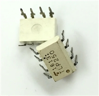
 TLP250光耦合器:资料手册参数分析

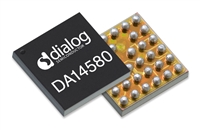
 DA14580 低功耗蓝牙系统级芯片(SoC):资料手册参数分析

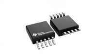
 INA226 高精度电流和功率监控器:资料手册参数分析

 SI2302 N沟道MOSFET:资料手册参数分析
