Data Sheet
ADuM3223/ADuM4223
SPECIFICATIONS
ELECTRICAL CHARACTERISTICS—5 V OPERATION
All voltages are relative to their respective ground. 4.5 V ≤ VDD1 ≤ 5.5 V, 4.5 V ≤ VDD2 ≤ 18 V, unless stated otherwise. All minimum/
maximum specifications apply over TJ = −40°C to 125°C. All typical specifications are at TJ = 25°C, VDD1 = 5 V, VDD2 = 12 V. Switching
specifications are tested with CMOS signal levels.
Table 1.
Parameter
Symbol
Min
Typ
Max
Unit
Test Conditions
DC SPECIFICATIONS
Input Supply Current, Quiescent
Output Supply Current, Per Channel, Quiescent
Supply Current at 1 MHz
VDD1 Supply Current
VDDA/VDDB Supply Current
Input Currents
Logic High Input Threshold
Logic Low Input Threshold
Logic High Output Voltages
Logic Low Output Voltages
Undervoltage Lockout, VDD2 Supply
Positive Going Threshold
Negative Going Threshold
Hysteresis
IDDI(Q)
IDDO(Q)
1.4
2.3
2.4
3.2
mA
mA
IDD1(Q)
IDDA/IDDB(Q)
IIA, IIB
VIH
VIL
1.6
5.6
+0.01
2.5
8.0
+1
mA
mA
µA
V
V
V
Up to 1 MHz, no load
Up to 1 MHz, no load
0 ≤ VIA, VIB ≤ VDD1
−1
0.7 × VDD1
0.3 × VDD1
0.15
VOAH, VOBH
VOAL, VOBL
VDD2 – 0.1
VDD2
0.0
IOx = −20 mA, VIx = VIxH
IOx = +20 mA, VIx = VIxL
V
VDD2UV+
VDD2UV−
VDD2UVH
VDD2UV+
VDD2UV−
VDD2UVH
VDD2UV+
VDD2UV−
VDD2UVH
IOA(SC), IOB(SC)
ROA, ROB
ROA, ROB
4.1
3.6
0.5
6.9
6.2
0.7
10.5
9.6
0.9
4.0
1.1
0.6
4.4
V
V
V
V
V
V
V
V
V
A
Ω
Ω
A-grade
A-grade
A-grade
B-grade
B-grade
B-grade
C-grade
C-grade
C-grade
3.2
5.7
Positive Going Threshold
Negative Going Threshold
Hysteresis
Positive Going Threshold
Negative Going Threshold
Hysteresis
7.4
11.1
8.9
2.0
Output Short-Circuit Pulsed Current1
Output Pulsed Source Resistance
Output Pulsed Sink Resistance
SWITCHING SPECIFICATIONS
Pulse Width2
Maximum Data Rate3
Propagation Delay4
VDD2 = 12 V
VDD2 = 12 V
VDD2 = 12 V
PW
50
1
26
30
ns
MHz
ns
CL = 2 nF, VDD2 = 12 V
CL = 2 nF, VDD2 = 12 V
tDHL, tDLH
tDHL, tDLH
tPSK
38
42
49
54
12
5
CL = 2 nF, VDD2 = 12 V; see Figure 20
CL = 2 nF, VDD2 = 4.5 V; see Figure 20
CL = 2 nF, VDD2 = 12 V; see Figure 20
CL = 2 nF, VDD2 = 12 V; see Figure 20
CL = 2 nF, VDD2 = 4.5 V; see Figure 20
CL = 2 nF, VDD2 = 12 V; see Figure 20
VDD2 = 12 V
ADuM3223A/ADuM4223A
Propagation Delay Skew5
Channel-to-Channel Matching6
ns
ns
tPSKCD
tPSKCD
tR/tF
1
ns
1
7
ns
Output Rise/Fall Time (10% to 90%)
Dynamic Input Supply Current Per Channel
Dynamic Output Supply Current Per Channel
Refresh Rate
6
12
18
ns
IDDI(D)
IDDO(D)
fr
0.05
1.65
1.2
mA/Mbps
mA/Mbps
Mbps
VDD2 = 12 V
1 Short-circuit duration less than 1 µs. Average power must conform to the limit shown under the Absolute Maximum Ratings.
2 The minimum pulse width is the shortest pulse width at which the specified timing parameter is guaranteed.
3 The maximum data rate is the fastest data rate at which the specified timing parameter is guaranteed.
4 tDLH propagation delay is measured from the time of the input rising logic high threshold, VIH, to the output rising 10% level of the VOx signal. tDHL propagation delay is
measured from the input falling logic low threshold, VIL, to the output falling 90% threshold of the VOx signal. See Figure 20 for waveforms of propagation delay
parameters.
5 tPSK is the magnitude of the worst-case difference in tDLH and/or tDHL that is measured between units at the same operating temperature, supply voltages, and output
load within the recommended operating conditions. See Figure 20 for waveforms of propagation delay parameters.
6 Channel-to-channel matching is the absolute value of the difference in propagation delays between the two channels.
Rev. 0| Page 3 of 20


 MAX6675资料手册参数详解、引脚配置说明

 LM258引脚图及功能介绍、主要参数分析

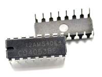
 CD4052资料手册参数详解、引脚配置说明

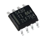
 一文带你了解TPS5430资料手册分析:参数介绍、引脚配置说明
