ADP3302
APPLICATION INFORMATION
To limit the maximum junction temperature to 125°C, maxi-
mum ambient temperature must be lower than:
anyCAP™
The ADP3302 is an easy to use dual low dropout voltage
regulator. The ADP3302 requires only a very small 0.47 µF bypass
capacitor on the outputs for stability. Unlike the conventional
LDO designs, the ADP3302 is stable with virtually any type of
capacitors (anyCAP™) independent of the capacitor’s ESR
(Effective Series Resistance) value.
TAMAX = 125°C ؊ 43.6°C = 81.4°C
PRINTED CIRCUIT BOARD LAYOUT CONSIDERATION
All surface mount packages rely on the traces of the PC board to
conduct heat away from the package.
In standard packages the dominant component of the heat
resistance path is the plastic between the die attach pad and the
individual leads. In typical thermally enhanced packages one or
more of the leads are fused to the die attach pad, significantly
decreasing this component. However, to make the improvement
meaningful, a significant copper area on the PCB has to be
attached to these fused pins.
Capacitor Selection
Output Capacitors: As with any micropower device, output
transient response is a function of the output capacitance. The
ADP3302 is stable with a wide range of capacitor values, types
and ESR (anyCAP™). A capacitor as low as 0.47 F is all that
is needed for stability. However, larger capacitors can be used if
high output current surges are anticipated. The ADP3302 is
stable with extremely low ESR capacitors (ESR ≈ 0), such as
multilayer ceramic capacitors (MLCC) or OSCON.
The ADP3302’s patented thermal coastline lead frame design
uniformly minimizes the value of the dominant portion of the
thermal resistance. It ensures that heat is conducted away by all
pins of the package. This yields a very low 96°C/W thermal
resistance for an SO-8 package, without any special board lay-
out requirements, relying just on the normal traces connected to
the leads. The thermal resistance can be decreased by, approxi-
mately, an additional 10% by attaching a few square cm of
copper area to the two VIN pins of the ADP3302 package.
Input Bypass Capacitor: An input bypass capacitor is not
required. However, for applications where the input source is
high impedance or far from the input pins, a bypass capacitor is
recommended. Connecting a 0.47 F capacitor from the input
pins (Pins 5 and 8) to ground reduces the circuit’s sensitivity to
PC board layout.
Low ESR capacitors offer better performance on a noisy supply;
however, for less demanding requirements a standard tantalum
or aluminum electrolytic capacitor is adequate.
It is not recommended to use solder mask or silkscreen on the
PCB traces adjacent to the ADP3302 pins since it will increase
the junction to ambient thermal resistance of the package.
Thermal Overload Protection
Shutdown Mode
The ADP3302 is protected against damage due to excessive
power dissipation by its thermal overload protection circuit,
which limits the die temperature to a maximum of 165°C.
Under extreme conditions (i.e., high ambient temperature and
power dissipation) where die temperature starts to rise above
165°C, the output current is reduced until the die temperature
has dropped to a safe level. The output current is restored when
the die temperature is reduced.
Applying a TTL high signal to the shutdown pin or tying it to
the input pin will turn the output ON. Pulling the shutdown pin
down to a TTL low signal or tying it to ground will turn the
output OFF. Outputs are independently controlled. In shutdown
mode, quiescent current is reduced to less than 2 A.
Error Flag Dropout Detector
The ADP3302 will maintain its output voltage over a wide
range of load, input voltage and temperature conditions. If
regulation is lost, for example, by reducing the supply voltage
below the combined regulated output and dropout voltages, the
ERRor flag will be activated. The ERR output is an open
collector, which will be driven low.
Current and thermal limit protections are intended to protect
the device against accidental overload conditions. For normal
operation, device power dissipation should be externally limited
so that junction temperatures will not exceed 125°C.
Calculating Junction Temperature
Device power dissipation is calculated as follows:
Once set, the ERRor flag’s hysteresis will keep the output low
until a small margin of operating range is restored, either by
raising the supply voltage or reducing the load.
PD = (VIN – VOUT1) ILOAD1 + (VIN – VOUT2) ILOAD2 + (VIN) IGND
Where ILOAD1 and ILOAD2 are Load currents on Outputs 1 and 2,
A single ERR pin serves both regulators in the ADP3302 and
indicates that one or both regulators are on the verge of losing
regulation.
IGND is ground current, VIN and VOUT are input and output
voltages respectively.
Assuming ILOAD1 = ILOAD2 = 100 mA, IGND = 2 mA, VIN = 7.2 V
and VOUT1 = VOUT2 = 5.0 V, device power dissipation is:
APPLICATION CIRCUIT
Dual Post Regulator Circuit for Switching Regulators
The ADP3302 can be used to implement a dual 3 V/100 mA
post regulator power supply from a 1 cell Li-Ion input (Figure
20). This circuit takes 2.5 V to 4.2 V as the input and delivers
dual 3 V/100 mA outputs. Figure 21 shows the typical efficiency
curve.
PD = (7.2 V – 5 V) 100 mA + (7.2 V – 5 V) 100 mA + (7.2 V)
2 mA = 0.454 W
The proprietary thermal coastline lead frame used in the
ADP3302 yields a thermal resistance of 96°C/W, which is signi-
ficantly lower than a standard 8-pin SOIC package at 170°C/W.
Junction temperature above ambient temperature will be
approximately equal to:
For ease of explanation, let’s partition the circuit into the
ADP3000 step-up regulator section and the ADP3302 low
dropout regulation section. Furthermore, let’s divide the operation
of this application circuit into the following three phases.
0.454 W ؋
96°C/W = 43.6°C
REV. 0
–7–


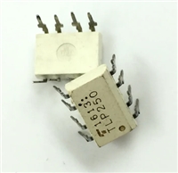
 TLP250光耦合器:资料手册参数分析

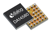
 DA14580 低功耗蓝牙系统级芯片(SoC):资料手册参数分析

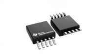
 INA226 高精度电流和功率监控器:资料手册参数分析

 SI2302 N沟道MOSFET:资料手册参数分析
