
 5秒后页面跳转

| 生命周期: | Obsolete | 零件包装代码: | SOIC |
| 包装说明: | SOP-8 | 针数: | 8 |
| Reach Compliance Code: | unknown | ECCN代码: | EAR99 |
| HTS代码: | 8542.39.00.01 | 风险等级: | 5.69 |
| 最大输入电压: | 22 V | 最小输入电压: | 3 V |
| JESD-30 代码: | R-PDSO-G8 | 长度: | 4.9 mm |
| 功能数量: | 1 | 输出次数: | 2 |
| 端子数量: | 8 | 工作温度TJ-Max: | 125 °C |
| 工作温度TJ-Min: | -40 °C | 封装主体材料: | PLASTIC/EPOXY |
| 封装代码: | SOP | 封装形状: | RECTANGULAR |
| 封装形式: | SMALL OUTLINE | 认证状态: | Not Qualified |
| 调节器类型: | FIXED POSITIVE MULTIPLE OUTPUT LDO REGULATOR | 座面最大高度: | 1.75 mm |
| 表面贴装: | YES | 端子形式: | GULL WING |
| 端子节距: | 1.27 mm | 端子位置: | DUAL |
| 宽度: | 3.9 mm | Base Number Matches: | 1 |
| 型号 | 品牌 | 描述 | 获取价格 | 数据表 |
| ADP3302AR-3.2 | ROCHESTER | DUAL OUTPUT, FIXED POSITIVE LDO REGULATOR, PDSO8, SOP-8 |
获取价格 |

|
| ADP3302AR-3.3 | ADI | IC VREG DUAL OUTPUT, FIXED POSITIVE LDO REGULATOR, PDSO8, SOP-8, Fixed Positive Multiple O |
获取价格 |
|
| ADP3302AR3-REEL | ADI | IC VREG DUAL OUTPUT, FIXED POSITIVE LDO REGULATOR, PDSO8, SOIC-8, Fixed Positive Multiple |
获取价格 |
|
| ADP3302AR4 | ADI | High Precision anyCAP⑩ Dual Low Dropout Linea |
获取价格 |
|
| ADP3302AR4-REEL | ADI | 暂无描述 |
获取价格 |
|
| ADP3302AR5 | ADI | High Precision anyCAP⑩ Dual Low Dropout Linea |
获取价格 |
|
 MAX485 RS-485/RS-422收发器资料手册参数分析

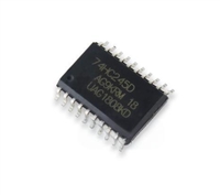 74HC245八路双向总线收发器:资料手册参数分析
 CD4053模拟多路复用器/解复用器:资料手册参数分析
 CD4011双4位二进制计数器:资料手册参数分析
工作时间:9:00-21:00
CEO邮箱:ceo@jiepei.com
投诉邮箱:tousu@jiepei.com


 浙公网安备 33010502006866号 浙ICP备10014259号-119
营业执照ICP证
浙公网安备 33010502006866号 浙ICP备10014259号-119
营业执照ICP证


