ADM1052
“HICCUP MODE” FAULT PROTECTION
GENERAL DESCRIPTION
Hiccup mode fault protection is a simple method of protecting
the external power device without the added cost of external
sense resistors or a current sense pin on the ADM1052. In the
event of a short-circuit condition at the output, the output
voltage will fall. When the output voltage of a channel falls 20%
below the nominal voltage, this is sensed by the hiccup com-
parator and the channel will go into hiccup mode, where the
enable signal to the control amplifier is pulsed on and off with a
1:40 duty cycle.
The ADM1052 is a dual, precision, voltage regulator controller
intended for power rail generation and active bus termination on
personal computer motherboards. It contains a precision 1.2 V
bandgap reference and two channels consisting of control amp-
lifiers driving external power devices. Both channels have an
output of nominally 2.525 V. Each channel has a shutdown
input to turn off amplifier output and protection circuitry for
the external power device.
The ADM1052 operates from a 12 V VCC supply. The output is
disabled until VCC climbs above the reset threshold (6 V–9 V). The
output from the ADM1052 is used to drive external N-channel
MOSFETs, operating as source-followers. This has the advan-
tage that N-channel devices are cheaper than P-channel devices
of similar performance, and the circuit is easier to stabilize than
one using P-channel devices in a common-source configuration.
To prevent the device inadvertently going into hiccup mode
during power-up or during channel enabling, the hiccup mode is
held off for approximately 60 ms on both channels. By this time
the output voltage should have reached its correct value. In the
case of power-up, the hold-off period starts when VCC reaches the
power-on reset threshold of 6 V–9 V. In the case of channel
enabling, the hold-off period starts when SHDN is taken high.
Note that the hold-off timeout applies to both channels even if
only one channel is disabled/enabled.
The external power devices are protected by a “Hiccup Mode”
circuit that operates if the circuit goes out of regulation due to
an output short-circuit. In this case the power device is pulsed
on/off with a 1:40 duty cycle to limit the power dissipation until
the fault condition is removed.
As the 3.3 V input to the drain of the MOSFET is not moni-
tored, it should ideally rise at the same or a faster rate than VCC
At the very least it must be available in time for VOUT to reach its
final value before the end of the power-on delay. If the output
.
CIRCUIT DESCRIPTION
voltage is still less than 80% of the correct value after the power-
on delay, the device will go into hiccup mode until the output
voltage exceeds 80% of the correct value during a hiccup mode
on-period. Of course, if there is a fault condition at the output
during power-up, the device will go into hiccup mode after
the power-up delay and remain there until the fault condition
is removed.
CONTROL AMPLIFIERS
The reference voltage is amplified and buffered by the control
amplifiers and external MOSFETs, the output voltage of each
channel being determined by the feedback resistor network
between the sense input and the inverting input of the con-
trol amplifier.
A power-on reset circuit disables the amplifier output until VCC
has risen above the reset threshold (6 V–9 V).
The effect of power-on delay is illustrated in Figure 2, which
shows an ADM1052 being powered up with a fault condition.
The output current rises to a very high value during the power-
on delay, the device goes into hiccup mode, and the output is
pulsed on and off at 1:40 duty cycle. When the fault condition is
removed, the output voltage recovers to its normal value at the
end of the hiccup mode off period.
Each amplifier output drives the gate of an N-channel power
MOSFET, whose drain is connected to the unregulated supply
input and whose source is the regulated output voltage, which is
also fed back to the appropriate sense input of the ADM1052.
The control amplifiers have high current-drive capability so that
they can quickly charge and discharge the gate capacitance of
the external MOSFET, thus giving good transient response to
changes in load or input voltage.
The load current at which the ADM1052 will go into hiccup
mode is determined by three factors:
• The input voltage to the drain of the MOSFET, VIN
• The output voltage VOUT (–20%)
SHUTDOWN INPUTS
Each channel has a separate shutdown input, which may be
controlled by a logic signal and allows the output of the regula-
tor to be turned on or off. If the shutdown input is held high or
not connected, the regulator operates normally. If the shutdown
input is held low, the enable input of the control amplifier is turned
off and the amplifier output goes low, turning off the regulator.
• The on-resistance of the MOSFET, RON
I
HICCUP = (VIN – (0.8 × VOUT))/RON
It should be emphasized that the hiccup mode is not intended as
a precise current limit but as a simple method of protecting the
external MOSFET against catastrophic fault conditions such as
output short circuits.
–6–
REV. A


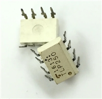
 TLP250光耦合器:资料手册参数分析

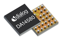
 DA14580 低功耗蓝牙系统级芯片(SoC):资料手册参数分析

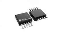
 INA226 高精度电流和功率监控器:资料手册参数分析

 SI2302 N沟道MOSFET:资料手册参数分析
