AD8170/AD8174
AD8170A/AD8174A
Parameter
Conditions
Min
Typ
Max
Units
INPUT CHARACTERISTICS
Input Resistance
(+) Switch Input
(–) Buffer Input
Channel Enabled (R Package)
Channel Disabled (R Package)
1.7
100
1.1
1.1
±3.3
56
MΩ
Ω
pF
pF
V
Input Capacitance
Input Voltage Range
Input Common-Mode Rejection Ratio
+CMRR, ∆VCM = 1 V
–CMRR, ∆VCM = 1 V
51
50
dB
dB
52
OUTPUT CHARACTERISTICS
Output Voltage Swing
RL = 1 kΩ, TMIN–TMAX
RL = 150 Ω, TMIN–TMAX
RL = 10 Ω
±4.0
±3.5
±4.26
±4.0
50
180
10
V
V
Output Current
Short Circuit Current
Output Resistance
mA
mA
mΩ
MΩ
pF
Enabled
Disabled (AD8174)
Disabled (AD8174)
10
7.5
Output Capacitance
POWER SUPPLY
Operating Range
±4
58
55
52
50
±6
V
Power Supply Rejection Ratio
Power Supply Rejection Ratio
Quiescent Current
+PSRR
–PSRR
+VS = +4.5 V to +5.5 V, –VS = –5 V
TMIN–TMAX
–VS = –4.5 V to –5.5 V, +VS= +5 V
TMIN–TMAX
All Channels “ON”, TMIN–TMAX
AD8174 Disabled, TMIN–TMAX
AD8174 Shutdown, TMIN–TMAX
66
58
dB
dB
dB
dB
mA
mA
mA
8.7/9.7
4.1
1.5
11/13
5
2.5
OPERATING TEMPERATURE RANGE
NOTES
–40
+85
°C
1Shutdown (SD) and ENABLE pins are grounded (AD8174). IN0 (or IN2) = +0.5 V dc, IN1 (or IN3) = –0.5 V dc. SELECT (A0 or A1 for AD8174) input is
driven with 0 V to +5 V pulse. Measure transition time from 50% of SELECT (A0 or A1) input value (+2.5 V) and 10% (or 90%) of the total output voltage transi-
tion from IN0 (or IN2) channel voltage (+0.5 V) to IN1 (or IN3 = –0.5 V) or vice versa.
2AD8174 only. Shutdown (SD) pin is grounded. ENABLE pin is driven with 0 V to +5 V pulse (5 ns rise and fall times). State of A0 and A1 logic inputs determines
which channel is activated (i.e., if A0 = Logic 0 and A1 = Logic 1, then IN2 input is selected). Set IN0 (or IN2) = +0.5 V dc, IN1 (or IN3) = –0.5 V dc, and mea-
sure transition time from 50% of ENABLE pulse (+2.5 V) to 90% of the total output voltage change. In Figure 5, ∆tOFF is the disable time, ∆tON is the enable time.
3AD8174 only. ENABLE pin is grounded. Shutdown (SD) pin is driven with 0 V to +5 V pulse (5 ns rise and fall times). State of A0 and A1 logic inputs determines
which channel is activated (i.e., if A0 = Logic 1 and A1 = Logic O, then IN1 input is selected). Set IN0 (or IN2) = +0.5 V dc, IN1 (or IN3) = –0.5 V dc, and mea-
sure transition time from 50% of SD pulse (+2.5 V) to 90% of the total output voltage change. In Figure 6, ∆tOFF is the shutdown assert time, ∆tON is the shutdown
release time.
4All inputs are grounded. SELECT (A0 or A1 for AD8174) input is driven with 0 V to +5 V pulse. The outputs are monitored. Speeding the edges of the SELECT
(A0 or A1) pulse increases the glitch magnitude due to coupling via the ground plane.
5Bandwidth of the multiplexer is dependent upon the resistor feedback network. Refer to Table III for recommended feedback component values, which give the best
compromise between a wide and a flat frequency response.
6Select input(s) that is (are) not being driven (i.e., if SELECT is Logic 1, activated input is IN1; in AD8174, if A0 = Logic 0, A1 = Logic 1, activated input is IN2).
Drive all other inputs with VIN = 0.707 V rms, and monitor output at f = 5 MHz and 30 MHz; RL = 100 Ω (see Figure 13).
7AD8174 only. Shutdown (SD) pin is grounded. Mux is disabled, (i.e., ENABLE = Logic 1) and all inputs are driven simultaneously with VIN = 0.354 V rms. Out-
put is monitored at f = 5 MHz and 30 MHz; RL = 100 Ω. In this mode, the output impedance of the disabled mux is very high (typ 10 MΩ), and the signal couples
across the package; the load impedance and the feedback network determine the crosstalk. For instance, in a closed-loop gain of +1, r OUT ഡ 10 MΩ, in a gain of +2
(RF = RG = 549 Ω), rOUT = 1.1 kΩ (see Figure 14).
8AD8174 only. ENABLE pin is grounded. Mux is shutdown (i.e., SD = Logic 1), and all inputs are driven simultaneously with V IN = 0.354 V rms. Output is moni-
tored at f = 5 MHz and 30 MHz; RL = 100 Ω. (see Figure 14). The mux output impedance in shutdown mode is the same as the disabled mux output impedance.
9For Gain Accuracy expression, refer to Equation 4.
Specifications subject to change without notice.
Table II. AD8174 Truth Table
Table I. AD8170 Truth Table
A0
A1
ENABLE
SD
VOUT
SELECT
VOUT
0
1
IN0
IN1
0
1
0
1
X
X
0
0
1
1
X
X
0
0
0
0
1
X
0
0
0
0
0
1
IN0
IN1
IN2
IN3
HIGH Z, IS = 4.1 mA
HIGH Z, IS = 1.5 mA
REV. 0
–3–


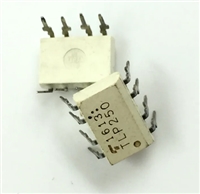
 TLP250光耦合器:资料手册参数分析

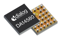
 DA14580 低功耗蓝牙系统级芯片(SoC):资料手册参数分析

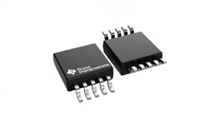
 INA226 高精度电流和功率监控器:资料手册参数分析

 SI2302 N沟道MOSFET:资料手册参数分析
